Segregation separates one part from the non-ideal influences of other parts. In electronic circuits, the dielectric is isolated by blocking direct current (DC). How does the isolated circuit operate in a larger electrical system? The answer to this question is the subject of this application report.
With the increasing number of products introduced by Texas Instruments and other suppliers, the transmission options for isolated signals have also increased, making designers more complex in product selection. This report describes the important features of the isolator and explains the differences and similarities between the products.
After reviewing the necessity of circuit isolation, we discussed three methods of dielectric signal transmission and analog to digital isolators and described and compared examples of each type of digital isolator.
2. Necessity of circuit isolation
The main reason for isolating the circuit is to protect the circuit from dangerous voltage and current damage. In the medical application example of Fig. 1, even a small amount of AC current may cause fatal injuries, so a barrier is needed to protect the patient. Isolation also protects sensitive circuits from high voltage damage in industrial applications. The industrial example of Figure 2 is only a high pressure measurement. Separating the sensor from the actual high voltage makes it possible to measure low voltage circuits.
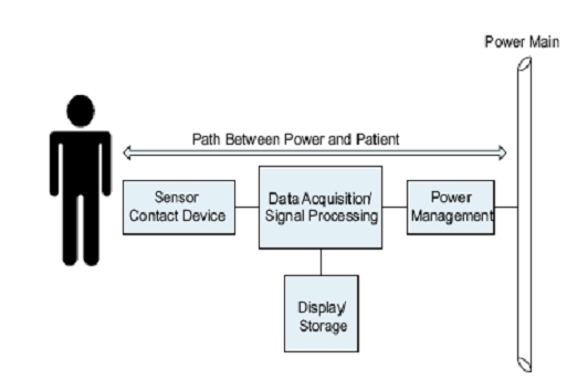
Figure 1: Possible circuit paths between the power supply and the patient.

Figure 2: Isolation between high and low voltage circuits.
The protection principle is to isolate high voltage potentials, which may appear in various systems or circuits, as shown in the cable application in Figure 3, where long distances can isolate one driver from the receiver. After such a long distance, the grounding may be at different voltages. By isolating, a voltage difference is created in the isolator rather than in the sensitive circuit.
Figure 3: Ground voltage difference between devices.
As shown in FIG. 4, the isolation interrupts the loop formed by the circuit path through high impedance relative to other circuit components. By interrupting the loop, noise voltages appear on the isolation layer rather than on the receiver or more sensitive components. The high level of the noise voltage can be coupled by an external current or voltage source (eg, inductive motor and lightning).

Figure 4: Ground loop between isolated disconnected nodes.
3. Circuit Isolator
Circuit isolators prevent low frequency currents between circuits while allowing analog or digital signal transmission through electromagnetic or optical links. Digital isolators transmit binary signals, and analog isolators transmit continuous signals on the isolation layer. In analog and digital isolators, the operating and peak voltage ratings as well as common-mode transient immunity are important characteristics of this isolation layer. When isolating digital signals, these important characteristics of the isolation circuit are input and output logic voltage levels, signal rates, data run lengths, and Auto-Protect responses.
Traditionally, transformers, capacitors, or photodiode transistors and discrete circuits are conditioned on input and output signals to meet special requirements. This method is effective, but it cannot be transferred from one application to another. Although this may hold analog isolators, there has been a new generation of digital isolators in the market that use innovative circuitry to isolate standard digital signals at data rates exceeding 100 Mbps DC. These universal digital isolators have their respective advantages and disadvantages. The following paragraphs will introduce various technologies and compare specific products with TI's new ISO72x series.
3.1 Optical Coupling Technology
Optical coupling technology is the transmission of light over a transparent insulating barrier (eg air gap) for isolation purposes. Figure 5 shows the main components of a digital isolator. The current driver uses a digital input and converts the signal into a current to drive a light emitting diode (LED). The output buffer converts the current output of the photodetector into a digital output.
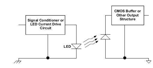
Figure 5: Basic optical coupling mechanism.
The main advantage of optical coupling technology is that light has inherent immunity to external electrons or magnetic fields, and optical coupling technology allows the use of constant information transmission. The shortcomings of optocouplers are mainly reflected in speed limitations, power consumption, and LED aging.
The maximum signal rate of an optocoupler depends on the speed at which the LED can turn on and off. From the current available products, the fastest optocoupler is HCPL-0723, which can reach 50Mbps signal rate.
The current-to-output ratio (CTR) from input to output is an important characteristic of optocouplers. LEDs typically require 10mA of input current for high-speed digital transmission. This ratio adjusts the current used to drive the LED and the current generated by the phototransistor. Over time, LEDs become more inefficient and require more current to produce the same level of brightness and the same level of phototransistor output current. In many digital isolators, the internal circuitry controls the LED drive current, and the user cannot compensate for the decreasing CTR. The advantages of LEDs have diminished, and the isolators are no longer as effective as they used to be over time.
3.2 Inductive coupling technology
Inductive coupling technology uses a changing magnetic field between two coils to communicate on a separate layer. The most common example is a transformer whose magnetic field size depends on the coil structure (number of turns/unit length) of the main and secondary windings, the dielectric constant of the magnetic core, and the current amplitude. Figure 6 shows a transformer with a signal conditioning circuit module.
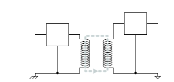
Figure 6: Inductive isolation.
The advantage of inductive coupling is that there may be common-mode differences and differential transmission characteristics. The careful design of the transformer allows the noise and signal frequencies to overlap, but exhibits high noise common mode impedance and signal low differential impedance. Another advantage is that signal energy transmission can be nearly 100% efficient, making low-power isolator possible.
The main drawback of inductive coupling technology is the magnetization of the external magnetic field (noise). Industrial applications often require magnetic isolation, such as motor control. Another drawback in digital transformer transmission is the length of data run. A signal converter transmits signals over a range of frequencies and amplitudes, and its distortion is acceptable. Data run length restrictions or clock coding are required to keep this signal within the available transformer bandwidth. Universal digital isolators using inductive coupling techniques require signal processing to transmit and reconstruct digital signals along with methods that transmit low-frequency signals (1 or 0 long characters). The Isoloop from NVE/Avago and the iCoupler from ADI (Analog Devices, USA) all use coding capabilities and provide a digital isolation solution that supports operation from DC to 100Mbps.
The ADuM1100 is an example of ADI's iCoupler technology. The ADuM1100 uses a basic transformer to transmit information over an isolation layer. This Isoloop technology (eg, HCPL-0900) uses a resistor network as shown in FIG. 7 to replace the secondary coil. The resistor consists of a GMR (giant magnetoresistive) material, which changes when the magnetic field is applied. The circuit senses changes in resistance and satisfies its conditions for output. When this technology was introduced to the market for the first time, AC performance was actually improved, exceeding the performance of existing optocouplers. Now, as ADI recently introduced more digital isolators and the introduction of TI's ISO72x family of devices, the performance of these Isoloop devices has been exceeded.
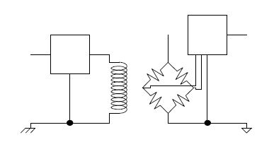
Figure 7: GMR structure diagram.
3.3 Capacitive coupling technology
Capacitive coupling technology uses a constantly changing electric field to transmit information on the isolation layer. The material between the capacitor plates is a dielectric separator and forms the isolation layer. The plate size, spacing between plates, and dielectric materials all determine electrical performance.
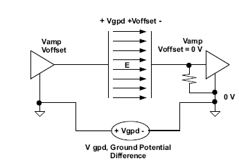
Figure 8: Capacitive coupling.
The benefits of using a capacitive isolation layer are high efficiency in size and energy transfer, as well as immunity to magnetic fields. The former makes it possible to integrate isolation circuits with low power consumption and low cost, while the latter makes it possible to operate in a saturated or high-density magnetic field environment.
The disadvantage of capacitive coupling is that it does not have differential signals and noise, and the signals share the same transmission channel, unlike transformers. This requires the signal frequency to be much higher than the noise expected frequency, so that the isolation capacitor exhibits a low impedance of the signal and a high impedance of the noise. After inductive coupling is used, capacitive coupling cannot transmit a steady state signal and requires clock coded data.
3.3.1 TI introduced the ISO721
TI's ISO72x series of isolator use capacitive coupling technology. Capacitive coupling solutions use proven, low-cost manufacturing processes with inherent immunity to magnetic fields.
In order to provide constant information transmission, the ISO72x uses a high signal rate and low signal rate channel for communication, as shown in Figure 9. The high signal rate channel is not encoded and it transmits data on a separate layer after single-ended to differential conversion. The low-signal-rate channel encodes data in a pulse-width modulation format and differentially transmits data over the isolation layer to ensure accurate communication at constant states (long characters of 1 and 0).
The differential transmission of single-ended logic signals on the isolation layer allows the use of low-level signals and small coupling capacitors. This presents a high impedance to common-mode noise and, through the receiver's common mode noise suppression, brings about excellent transient immunity, which is the main problem that signal capacitive coupling needs to solve.

Figure 9: Block diagram of ISO72x and ISO72xM.
3.4 Isolation performance
Three major standards validate the need for isolation protection, which are UL 1577, IEC 60747-5-2, and CSA, respectively. Although each standard is slightly different, it provides a standard for comparing isolation performance. Tests by IEC, UL, and CSA confirmed the voltage outside the dielectric breakdown between input and output. The use of these standards is very simple, because the test criteria and the isolation method are irrelevant. Figure 10 shows how the isolation test treats the isolator as a two-terminal device. Although there is a difference in the physical structure of each device, the isolation test is measured on the dielectric breakdown voltage.
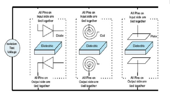
Figure 10: Isolation voltage test at both ends.
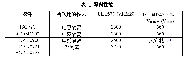
UL 1577, IEC 60747-5-2, IEC 61010-1, and CSA tested the ISO72x family of isolation performance. Table 1 shows the isolation performance of these five devices illustrating the three isolation techniques.
All three tests, namely UL, CSA, and IEC, tested the quality of the isolation layer. Both UL and CSA tests are stress tests that use a specified time set by the manufacturer to test dielectric breakdown voltage. Breakdown of the dielectric is a failure that occurs during this test. The IEC test uses a phenomenon known as partial discharge to detect voids in the dielectric. A large voltage is applied to the device, which is a function of the operating voltage defined by the manufacturer and then reduced to another voltage level, Vm. In this low voltage application, the device under test is subjected to ineffective partial discharge monitoring within the dielectric. These invalidities will result in the final breakdown of the entire dielectric.
3.5 Transient immunity
High slew rate (high frequency) transients can disrupt data transmission on one isolation layer. This isolation capacitor provides a channel as shown in Figure 11 that causes transient events to pass through the isolation layer and disrupt the output waveform. A Faraday shield can keep this part of the displacement current in the optocoupler or inductive coupler away from the important output structure.
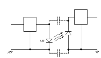
Figure 11: Spacer Capacitance.
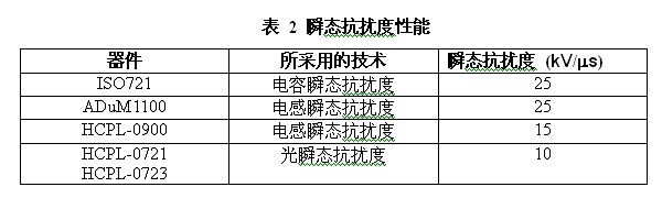
In capacitive coupling solutions, Faraday shield is not a viable solution. In addition to transients, Faraday shields also block the electric field used for data transmission. In order to provide transient immunity, the ISO72x series capacitive isolators transmit only fo signals (data signals that represent only the highest frequency energy in the signal). This allows a small coupling capacitor with a high noise frequency. Other noise comes from the differential technique of transmitting data on the isolation layer. Figure 9 shows the four signals passing through the capacitive isolation layer; two contain low signal rate information and the other two contain high signal rate information. By using differential techniques, any remaining common-mode transients through the isolation layer can be seen in the real and compensated signals, and the differential receiver rejects it. As shown in Table 2, the transient immunity of the ISO72x series is as high as all comparable devices up to 25 kV/us.
3.6 Automatic Protection
The data line circuit and the digital isolator need to pay attention to the output state of the input signal loss. Input loss may occur when the cable is disconnected or removed directly from the isolator input. Auto-protection refers to a deterministic or known output state under input loss conditions. The ISO72x family uses a periodic pulse to determine if the input structure is powered and is working. If the output of the isolator does not receive a pulse after 4 us, the output is set to a high state. The ADum1100 from ADI also integrates an automatic protection circuit in the output section of the IC. Avago Technologies' optical solutions (HCPL-0721 and -0723) do not mention auto-protection, and the inductive GMR solution (HCPL-0900) clearly describes the indeterminate nature of the output during power sequencing.
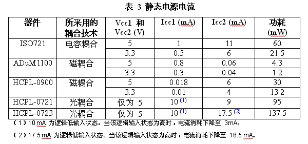
3.7 Power Consumption
In addition to the efficiency of signal transmission at the isolation layer, the design of the input and output conditioning circuits is most relevant to power consumption. As shown in Table 3, optocouplers consume more power than inductors or capacitors.
3.8 Reliability
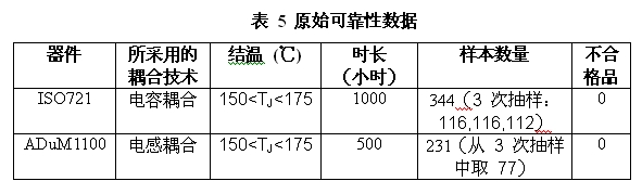
The mean time to failure (MTTF) is a standard measure of semiconductor device reliability. For digital isolators, this measurement represents the reliability of the integrated circuit and isolation mechanism. Table 4 shows the MTTF of an optical, inductive and capacitive digital isolator. Compared to inductors and optical solutions, ISO721 is very reliable.
The ADuM1100 reliability data sheet does not explicitly describe the MTTF, but it provides the results of a reliability test. Table 5 shows the parameters of the ISO721 and ADuM1100 reliability tests.

3.9 External Magnetic Field Immunity
Figure 12 compares the magnetic field immunity of the ADuM1100 and ISO72x (data not found for the HCPL-0900) . Relatively speaking, although both of these examples have a certain degree of immunity to magnetic fields, ISO72x offers a greater margin. As previously described, the optically coupled isolation layer circuit has an inherent magnetization immunity to the external magnetic field.

Figure 12: Sensitivity to an external magnetic field.
4. Summary of this article
Noise reduction and noise protection make isolators widely used in electronic circuits where those isolators interrupt the ground loop and isolate the ground voltage differential. Designers now have many options for digital signal isolation, including the TI's ISO72x family of key features such as signal rate, dielectric breakdown voltage, transient immunity, power consumption, magnetic field immunity, and reliability. All have performed well. Table 6 summarizes these characteristics of the examples discussed in this report.
bibliography
1. "electronic noise reduction technology system in the second edition," the authors: HW Ott;
2. "Electronic Design Compatibility Guide" Author: D Girke, B. Kimmel;.
3. "HCPL-0721 Product Manual", Avago Technologies;
4. "HCPL-0723 Product Manual", Avago Technologies;
5. "HCPL-0900 Product Manual", Avago Technologies;
6. Optocoupler Input Drive Circuit, AN3001 Fairchild Application Manual;
7. "ADuM1100 Product Specification Revision E", American Analog Devices Corporation;
8. "ISO72x Product Specification", TI (SLLS629);
9. "ISO72x Digital Isolator Magnetic Field Immunity" TI Application Report (SLLA181);
10. "sensor", January 1999 edition, "System Design Guide isolation device" by: P Pickering;
11. "40ns propagation delay CMOS optical coupler reliability product specification", July 2002 edition, Agilent Technologies (Avatech);
12. "Agilent HCPL-0900/0930/0931 High-Speed ​​Digital Optical Isolator Reliability Data Sheet", May 2005 Edition, Agilent Technologies (Avatech);
13. "ADuM1100Fab Transmission, Reliability Report", December 2002, Analog Devices, USA.
Double Sided PCB - the most popular type of PCB in the industry
While single-sided PCBs are simple and ideal to use when possible, many circuits require two sides. Double-sided PCB boards offer a wide variety of possibilities for circuit board designers because they have more surface area and flexibility when routing traces. Using two sides instead of one also allows for a smaller board size overall, which can be important when building small-scale, integrated devices.Double-sided PCB is one of the most common types of PCB. Moreover, the two-sided PCB and the single-sided PCB are basically the same to some extent. The difference is that the single-sided PCB has only one conductive surface. That is to say, the one-sided PCB has copper on one side of the board, but the two-sided PCB has conductive layer on each side. The dielectric layer is surrounded by the copper layer of the circuit and welding masks on both sides. Technically, single-sided circuit boards will not be copper plated in boreholes. Passing holes allow manufacturers to create traces on both sides that are adjacent to each other and connected between layers. PCB manufacturers use double-sided PCBs for products that require elementary to intermediate circuit complexity. This type of PCB does not provide as much circuit complexity or density as multi-layer PCB, but it is the most economical choice in many applications.
Nowadays, double-sided Printed Circuit Boards can be designed and manufactured in a variety of ways, including silver and gold surface treatment, high and low temperature and solder coating. This versatility enables them to power almost unlimited numbers of projects at cost-effective prices. Because of these advantages of double-sided PCB, double-sided PCB technology has become the most popular type of PCB in the industry.

What is Double-Sided PCB?
Strictly speaking, the Double-Sided PCB is one kind of the important PCB boards which is useful in PCB industry. They allow for the routing of traces around each other by jumping between a top and bottom layer by way of vias. Generally speaking, There are lines on both sides! The common PCBs can be seen such as, Rigid PCB , Flexible circuit board, Aluminum PCB and Metal Core PCB.
It need circuits on both sides. Via is the holes on boards, coated with metal and it can connect wires on both sides. Because the area of Double-sided PCB is twice as large as the Single-sided PCB, and because the wiring is interleaved, which is better suited for circuits that are more complex.
Someone may feel confused that if one Double-sided PCB, wires on both sides while Electronic parts only one side, is this a Double-sided board or a single onel? The answer is obvious. This kind of board is a Double-sided board, it's just install a component on the Double-sided board.So the question is, if a double-sided PCB has circuits on both sides, but only one side has electronic accessories, is it a double-sided PCB or a single-sided PCB? The answer is obvious. This kind of board is a double-sided circuit board. It only installs a component on the double-sided PCB.
Double sided circuit boards are one of the most popular types of PCBs as they enable manufacturers to produce more complex circuits, which can benefit uses in higher technology applications and electronics. There is an abundance of applications and electronics which double sided PCBs can be used in including: lighting systems, vending machines, amplifiers, car dashboards, and many more.
Double Layers PCB expands design capability and reduces physical sizes.

Double-Sided PCB material
The manufacturing base material of PCB is rigid glass fiber laminate. In the actual manufacturing process, many types of PCB materials can be used. Which material to use is determined by the PCB designer to meet electrical, temperature and other related characteristics. However, the standard material commonly used is fiberglass, which we usually call FR4.
FR, which technically stands for "flame retardant", does not mean specific material, but refers to material grade. However, it is a glass fiber reinforced epoxy laminate with flame retardant standard UL94V-0.
FR4 is the most common and typical choice of rigid PCB materials. Usually we classify them into three categories:
Normal Tg = Material melting point over 130 degrees Celsius
Medium Tg = Material melting point more than 150 degrees Celsius
High Tg = Material melting point more than 170 degrees Celsius
Double-Sided PCB construction

Double Sided PCB Layers


Benefits of Double Sided PCBs
Double-sided PCB is a widely used component in various applications, because it can achieve greater flexibility in designing more complex circuits. The following are some advantages of double sided PCB:
- Improving circuit density and complexity: By having conductive layers on both sides, the component space of double-sided PCB is twice as large as that of single-sided PCB. It can easily increase the density and complexity of the circuit.
- Double-sided PCB is widely used: Double-sided PCB has circuit complexity and can be used for many common electronic products at reasonable prices. Use double-sided PCB to make popular electronic products for daily use.
- More suitable for more complex projects: Double-sided PCB is the same size as single-sided PCB, but has twice the component space. Design more complex projects with the same amount of space.
- Cost-effective manufacturing: Double-sided PCB has the ability to be used in a large number of projects, and the price is lower than multi-layer PCB, avoiding paying extra costs.
- Provide more design possibilities: at relatively low cost, you can greatly expand the number of projects available for your functions and budget. Creating innovations that a single-tier PCB cannot achieve.
- Redirect the PCB current while keeping the top free: You can use the bottom of the double-sided PCB as grounding copper casting for sinking and output current.
Double sided PCB boards is different from Single-sided PCB.
Single-sided PCB is the basic one, the spare parts are concentrated in one side, and the circuit is concentrated on the other.Because the wires only appear on the one side of themso we called Single-sided PCB. Because the single-sided PCB has many strict restrictions on the design circuit (because only one side, the wiring cannot cross and must move around the individual path), so it only used on earlier circuits.
Single-sided PCB diagram mainly used Network Printing(Screen Printing), that is, resist on copper surface, After etching, mark the welding resistance, and then finish the hole and the shape of the part by punching.
Single sided printed circuit boards are widely used in many electronics whereas double sided circuit boards are often used in higher technology electronics.
Single sided printed circuit boards are commonly used in an array of electronics and applications, including: camera systems, printers, radio equipment, calculators, and much more.
Benefits of Single Sided PCBs
Single sided circuit boards are considered to be one of the best choices for a wide range of applications due to the advantages that it provides. Here are a few advantages of single sided printed circuit boards:
- The cost of manufacturing and producing single sided circuit boards are very cost-effective and affordable due to the simple and basic designs. These types of PCBs are widely understood by various manufacturers which makes single sided boards the best choice for circuit designs that are simple and low density.
- As single sided boards are less complex, there will undoubtedly be fewer problems during the manufacturing stage, which enables manufacturers to produce these boards at higher volumes and at faster speeds. Due to this, they are commonly used in many applications and electronics.
With higher volume orders, single sided circuit boards can be more affordable and available at reduced costs.
Double-Sided PCB Applications
Many of the electronics found in everyday life function on double-sided PCBs. Applications of double-sided PCBs include:
- Industrial controls
- Power supplies
- Converters
- Control relays
- Instrumentation
- Regulators
- UPS systems
- Power conversion
- HVAC
- LED lighting
- Hard drives
- Printers
- Phone systems
- Power monitoring
- Automotive dashboards
- Line reactors
- Test equipment
- Amplifiers
- Traffic systems
- Vending machines
Double-Sided PCB fabrication
Double Sided PCB Home Made DIY
DIY Double Sided PCB
Learn more about our products and services through the following links:
- Reflow double sided PCB
- A Collection of Questions on Double Sided PCB
- Advantages of Double Sided PCB
- Double Sided Metal Core PCB
- Double sided Rigid PCB
Double Sided PCB
2 Layer PCB,Double Sided Fr4 PCB,pcb prototype service,Double Layer PCB
JingHongYi PCB (HK) Co., Limited , https://www.pcbjhy.com