In recent years, the design difficulty of mobile communication antennas installed in mobile communication terminals has gradually increased. With the increase in the new communication method of LTE, the use of broadband is becoming more and more widespread. On the other hand, due to factors such as the increase in size of secondary batteries, the usable space (antenna/area) has been reduced. Therefore, the miniaturization of the antenna has become a top priority. However, if the antenna is miniaturized, it means that the impedance of the antenna will be lower than the input and output impedance of the RF circuit (50Ω system), which means that the RF circuit and the antenna impedance are integrated through the full communication bandwidth. is very difficult.
At present, when performing impedance integration, LC components such as an inductor (L) and a capacitor (C) are generally used. However, the LC component has a frequency characteristic, and the Q value of the antenna after the integrated impedance is degraded, and the frequency bandwidth is reduced.
Here, for materials that are difficult to exhibit in frequency characteristics during impedance conversion, a transformer mainly used in the low frequency field is exemplified. The transformer achieves the converted impedance by the ratio of the inductance (L value) of the two coils (transformer, coil) combined with the magnetic field, so the frequency characteristics in the ideal state cannot be guaranteed. So we consider using it in the integration of impedance.
There are three problems with using a transformer in an antenna for mobile communication.
1) Due to the "permeability of magnetic material ≒1" in the microwave frequency band, it is difficult to achieve a high coupling coefficient;
2) The small input impedance of the antenna will cause a large loss of transformer loss;
3) The antenna input impedance value will vary due to the frequency band.
Because of these problems, transformers have not been used in the impedance integration of mobile communication antennas until now. And we solved this problem through a unique method.
The coupling coefficient refers to a change in the two transformers constituting the transformer, the distance between the coils, and the shape dependence of the magnetic flux caused by the coil. Since the transformation ratio is controlled while maintaining a high coupling coefficient, the shape of the transformer and the coil are in a uniform state, and a structure in which the L value of each coil can be freely controlled is developed.
This structure is constructed in LTCC (Low Temperature Co-fired Ceramic) and can be made with a distance between the transformer and the coil of several tens of μm. The coupling coefficient of the transformer can be controlled to 0.7 or more even in the microwave band.
Connecting a high-frequency transformer to an antenna with a 10Ω impedance, the insertion loss (insertion loss) due to the material properties of the transformer itself is relatively larger than that of a high-frequency device connected to 50Ω. Therefore, a transformer having a large L value and an impedance component generally used in a low frequency is difficult to use at a high frequency.
In order to reduce this impedance component and maintain the transformation ratio, we have adopted the configuration of the high frequency transformer shown in Fig. 1. This configuration is the opposite of a normal transformer construction in that it completely reverses the ground connection port to the antenna connection port. Therefore, the transformation ratio as shown in Fig. 1 can be achieved. With this configuration, the mutual inductance M value due to the combination is reflected to the transformer, and the value of the coil L used in the transformer is reduced, since the impedance component IL of the high-frequency transformer can be suppressed to be small.
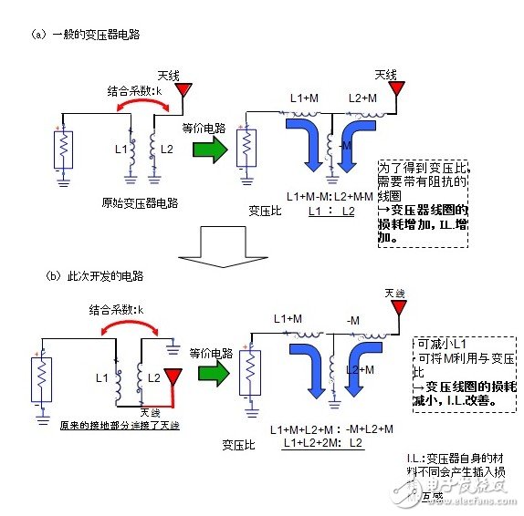
The communication bandwidth used in the mobile communication antenna is divided into a low field "lowband" and a high field "highband" by a limit of 1 GHz. In an open antenna, generally, the lowband is the fundamental wave of the antenna and the highband is the high frequency wave of the antenna. When the anti-integration function such as short pins is not installed inside the antenna, the impedance of the lowband is about 10Ω, and the impedance of the highband is about 19Ω.
If a transformer with a certain transformer ratio is installed in such an antenna, it is impossible to integrate only the impedance of one band. Therefore, for antenna transformers, the necessary design requirement is to adapt the transformation ratio to the impedance frequency characteristics of the antenna. This adaptation method is shown in Figure 2. It is an equivalent circuit that decomposes the ideal transformer part and parasitic component.
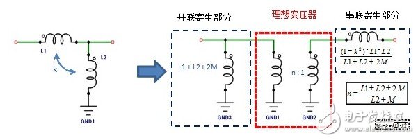
The parasitic components of the transformer structure developed this time are classified into two types: "series L" and "parallel L". Among them, the series parasitic component can be reduced by increasing the binding coefficient, and the parallel parasitic component may have a "binding coefficient = 1". In the high-frequency transformers with the necessary small L-value design, it is impossible to eliminate the influence of parallel parasitic components. However, the transformation ratio can be adapted to the impedance frequency characteristics of the antenna by controlling the value of such parallel parasitic components. The value of the parallel parasitic component can be controlled by switching the L value of the transformer coil. This time, we found a combination of the L value and the coupling coefficient K that can well control the parallel parasitic components.
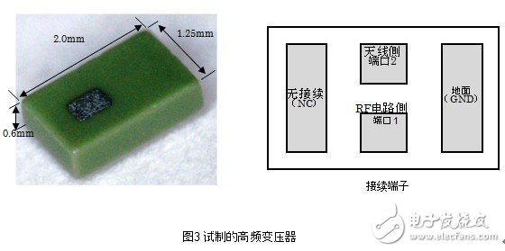
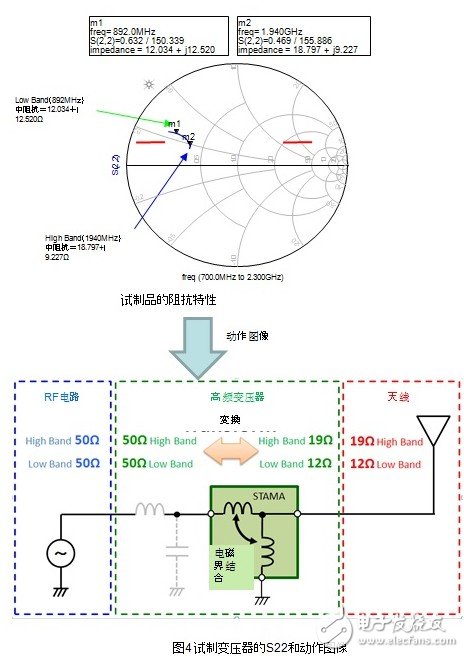
With the above-described structure, a high-frequency transformer was experimentally produced and evaluated for the purpose of simplifying the integration of the antenna group. The dimensions of the prototype are 2.0mm 1.25mm 0.6mm surface mount components (SMD) (Figure 3). A 50 Ω measuring device is connected to the RF circuit side of the test piece, and the impedance and animation of the antenna connection side are as shown in FIG. The prototype transformer converts lowband (892MHz) into 12→50Ω, and highband (1940MHz) is replaced by 19→50Ω.
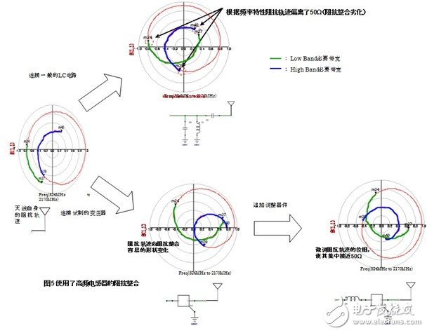
Connecting an ordinary LC circuit to an antenna makes impedance integration difficult under wide bandwidth conditions depending on frequency characteristics. In response to this situation, the high-frequency transformer of this trial is connected to the antenna, and both lowband and highband are converted into the most suitable impedance. That is to say, the impedance trajectory on the artisan map may change into a shape in which impedance integration is easy. The phase of the impedance trace is then fine-tuned by an external adjustment element, which may be very easily concentrated around 50 Ω. (Figure 5)
When the high-frequency transformer is installed in a communication terminal, what are the advantages, and the antenna characteristics are compared and evaluated in an environment where the installation is not performed.
Using the Sharp "ISW16SH" model on the market, the characteristics of the impedance integration in the LC circuit are compared and evaluated using the characteristics of the high-frequency transformer for impedance integration. (Image 6)
![]()
The ISW16SH model has a USB interface directly under the antenna section, and the electric field of the antenna is evaluated by connecting with the interface under strict conditions.
The results show that LC and high-frequency transformers are unlikely to achieve "S11"-6dB" (reflection loss 1.2dB) in the case of lowband. In the case of highband, the range of "S11"-6dB" is 300MHz if LC circuit is used, and 500MHz when using high frequency transformer, which achieves 66% improvement. (Fig. 6(c)). In addition, the integrated characteristics of the antennas in the LC circuit and the high-frequency transformer show "TotalEfficiency", and the high-frequency side of the lowband also has an improvement of 0.6 dB. (Fig. 6(d)). This improvement is due to the wide bandwidth and improved IL.
Next, the effectiveness of antenna miniaturization will be tested. In general, antennas have the property of improving the grounding distance. However, if the antenna occupies a large space (excluding the GND area), the mounting space of components other than the antenna is pressed. Miniaturization of the antenna and shrinking of the antenna space are imminent. When a part of the antenna space is occupied by the GND, the change in the antenna characteristics at this time is evaluated. The width of the antenna space is 52 mm, of which 13 mm is occupied by GND, and the characteristics of the lowband deteriorate, becoming the TotalEfficiency equivalent to the LC circuit (Fig. 7(b)). This means that the area of ​​the antenna space can actually be reduced by 25%.
![]()
In summary, it can be proved that the high-frequency transformer of this trial can change the characteristics of the antenna compared with the ordinary LC circuit. The transformer-to-voltage ratio of the high-frequency transformer adapts to the lowband and highband impedance of the antenna. Even in the full-band range, it can be said that stable impedance integration can be obtained.
We will productize the equipment developed this time. This device will be considered as a "third impedance integrated device" after the inductor and capacitor. This device is a passive component that uses a transformer. Like inductors and capacitors, it is not as competitive as active devices such as transfer switches, but it has a high affinity. It corresponds to the multi-functionality of the portable terminal, and the antenna must evolve in the future. We firmly believe that the device will contribute to this evolution in the future.
Description of Stacked D-Sub I/O Connectors
Antenk's connectors are designed for applications requiring multiple connector ports with limited PCB space
The condensed footprint of Antenk's dual port D-sub solution is available in four industry sizes, three connector spacing options, and six hardware configurations for one of the broadest stacked D-sub offerings on the market in standard and high-density variations.
Stacked D-sub I/O Connectors are designed for applications requiring multiple connector ports with limited PCB space. Two right angle D-sub connectors are stacked one on top of another, creating a single dual-port connector with a very condensed footprint.
Features of Stacked D-Sub I/O Connectors
Available in four industry standard sizes:
Standard Density : 9, 15, 25, 37
Available in three connector spacing options: 0.625", 0.750", 0.900"
Available in six hardware configurations
High-temperature UL94 V-0 thermoplastic (260°C process temp)
High performance stamped contacts
Applications of Stacked D-Sub I/O Connectors
Communications
Instrumentation
Medical
Computers/peripherals
Commercial industry
Test labs
Gaming industry
Range of of Stacked D-Sub I/O Connectors
Male Stacked D sub Connector
Female Stacked D sub ConnectorStandard Density Stacked D sub Connector
High Density Stacked D sub Connector
Dual-Port Stacked D-Sub Connectors
Stacked D-Sub I/O Connectors
Dual Port (Stacked) D Sub,,Stacked D Sub I/O Connectors,Dual-Port Stacked D-Sub Connectors,Male Stacked D sub Connector, Female Stacked D sub Connector, Standard Stacked D sub Connector, High Density Stacked D sub Connector
ShenZhen Antenk Electronics Co,Ltd , https://www.antenk.com