Abstract: When using a Dallas Semiconductor high-speed microcontroller with external memory, noise from P0 switching could couple to ALE. With careful board layout and a good understanding of induced noise on a mulTIplexed address / data bus, these problems can be minimized. This applicaTIon note looks at the DS80C320 high-speed microcontroller when accessing external memory.
OverviewThe 8051 architecture allows for external program and data access through the use of Port 0 and Port 2 as an external memory interface. The 8051 architecture mulTIplexes the data and LSB of address on Port 0, requiring a 74373 latch for demulTIplexing. This means that Port 0 will be directly connected to at least two devices. More devices may be placed on the bus if an external data SRAM or memory-mapped peripherals are used.
Because Port 0 must switch quickly between address and data, it requires strong current drive characteristics. Unfortunately, the high instantaneous current requirements of quickly switching all the pins of Port 0 can induce noise on the ALE signal. In some instances, this noise can interfere with program and data accesses by causing the external hardware to latch an incorrect address. This is a relatively rare occurrence, and most designers will not encounter it. The magnitude of this problem is directly related to several issues associated with both the system and software. Devices which do not access external memory via Port 0 and Port 2 will not experience this problem.
This application note will discuss ways the system designer can reduce the effects of Port 0 switching on device operation. It is applicable to any ROMless 8051 microcontroller which accesses external memory via Port 0 and Port 2, including the DS80C310 and DS80C320. It is also applicable to any microcontroller with internal program memory that accesses external memory.
ALE Noise GenerationUnder certain system conditions, noise induced on ALE can cause an incorrect LSB address to be latched when using the multiplexed address / data bus. The noise, as seen in Figure 1, is generated by the highspeed switching of Port 0 when the processor stops driving a memory address and begins driving data during a MOVX write. The noise pulse can, under the right conditions, rise above the VIH input threshold of TTL, LS, FS and HCT logic. In this case, the 74373 latch may be falsely triggered, latching an incorrect address and disturb the LSB address of the MOVX write.
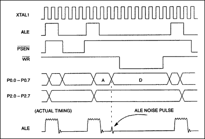
Figure 1. Data memory write (ideal timing).
Figure 2 shows a system diagram of how the noise pulse is generated. The noise pulse is produced when the processor drives a Port 0 pin with a high address (see "A" in Figure 1) followed by a low for data (see "D "in Figure 1). The device must sink a relatively large amount of current on each pin (IB) to take the line from a high to low state. It is obvious that the more pins which change from a high to a low, the larger the noise. The worst case will be during a MOVX write instruction with an LSB address of FF (Hex) and a data byte of 00 (Hex). Because all eight port pins are switching simultaneously, the maximum amount of current will be drawn into the microcontroller. The combined inductance and resistance both inside the processor and in the system result in the processor internal ground rising above the system ground. This in turn induces the noise seen on ALE. The case of a MOVX read does not involve the sinking of current by the processor and should not induce significant noise on the ALE signal. System elements which have a direct relationship to the magnitude of the noise are: Port 0 bus capacitance. System ground inductance (L2) and resistance (R2). System supply voltage (VCC).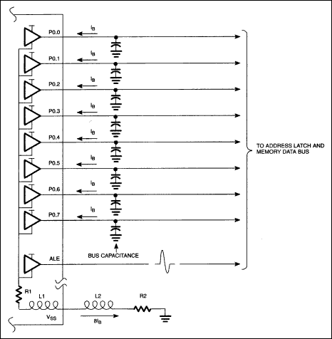
Figure 2. ALE noise source.
Noise Reduction There are several techniques that can be used to minimize the effect of Port 0 switching on ALE noise. Reducing bus capacitance reduces the energy required to be discharged which results in lower peak currents and reduced peak voltages in the noise pulse. Reducing the external ground resistance and inductance also reduces the noise level by reducing the resistive and inductive voltage drop.
The supply voltage is also directly proportional to the voltage level of the noise pulse. Maintaining VCC within recommended specifications will limit the noise voltage level.
Adding low impedance resistors in series with Port 0, as seen in Figure 3, reduces the noise level by limiting the peak current drawn into the microcontroller. Care must be taken to verify that these resistors do not adversely effect the slew rate or final input voltage level to the memory as the processor writes to external memory. Values ​​in the range of 50Ω to 150Ω can generally be used without disturbing write cycle times. Actual values ​​for the series resistance should be verified in the end system.
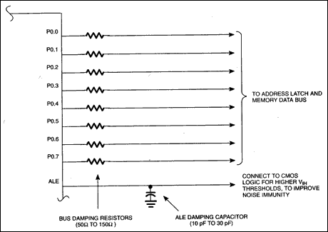
Figure 3. Noise reduction.
Use of a capacitor on the ALE signal line will also significantly reduce the noise pulse. Again, values ​​must be verified in the system, with care used in not reducing the slew rate of the ALE signal to a point that memory access is no longer valid . Generally a capacitance of between 10 and 30pF is sufficient to reduce the noise level without effecting normal system operation.
Input ThresholdsThe simplest and most reliable method of eliminating the address latch related noise is to select a logic family with a high input threshold. Standard TTL, LS, FS, and HCT logic parts have a VIH threshold of approximately 2.0 volts. HC (High- Speed ​​CMOS) or AC (Advanced CMOS) logic, on the other hand, has a VIH of approximately 3.5 volts at a supply voltage of 5 volts. The higher threshold level of the HC or AC CMOS logic increases the noise immunity by approximately 1.5 volts . This is generally all that is needed to prevent the undesired latching by ALE.
One disadvantage of using CMOS logic is that it is slower than other logic families. Propagation delays through CMOS logic are generally in the range of 18 ns for HC and 10 ns for AC, compared with 2 to 4 ns for FS logic when using a supply of 5 volts. For slower microcontrollers such as the DS5000, DS5001, and DS5002, the propagation delay is usually not an issue because of the slow clock rate. Faster microcontrollers such as the High-Speed ​​Microcontrollers should carefully consider the timing effects of slower logic . In any event, testing should be done in the final application to verify the effects using slower CMOS logic.
OverviewThe 8051 architecture allows for external program and data access through the use of Port 0 and Port 2 as an external memory interface. The 8051 architecture mulTIplexes the data and LSB of address on Port 0, requiring a 74373 latch for demulTIplexing. This means that Port 0 will be directly connected to at least two devices. More devices may be placed on the bus if an external data SRAM or memory-mapped peripherals are used.
Because Port 0 must switch quickly between address and data, it requires strong current drive characteristics. Unfortunately, the high instantaneous current requirements of quickly switching all the pins of Port 0 can induce noise on the ALE signal. In some instances, this noise can interfere with program and data accesses by causing the external hardware to latch an incorrect address. This is a relatively rare occurrence, and most designers will not encounter it. The magnitude of this problem is directly related to several issues associated with both the system and software. Devices which do not access external memory via Port 0 and Port 2 will not experience this problem.
This application note will discuss ways the system designer can reduce the effects of Port 0 switching on device operation. It is applicable to any ROMless 8051 microcontroller which accesses external memory via Port 0 and Port 2, including the DS80C310 and DS80C320. It is also applicable to any microcontroller with internal program memory that accesses external memory.
ALE Noise GenerationUnder certain system conditions, noise induced on ALE can cause an incorrect LSB address to be latched when using the multiplexed address / data bus. The noise, as seen in Figure 1, is generated by the highspeed switching of Port 0 when the processor stops driving a memory address and begins driving data during a MOVX write. The noise pulse can, under the right conditions, rise above the VIH input threshold of TTL, LS, FS and HCT logic. In this case, the 74373 latch may be falsely triggered, latching an incorrect address and disturb the LSB address of the MOVX write.
Figure 1. Data memory write (ideal timing).
Figure 2 shows a system diagram of how the noise pulse is generated. The noise pulse is produced when the processor drives a Port 0 pin with a high address (see "A" in Figure 1) followed by a low for data (see "D "in Figure 1). The device must sink a relatively large amount of current on each pin (IB) to take the line from a high to low state. It is obvious that the more pins which change from a high to a low, the larger the noise. The worst case will be during a MOVX write instruction with an LSB address of FF (Hex) and a data byte of 00 (Hex). Because all eight port pins are switching simultaneously, the maximum amount of current will be drawn into the microcontroller. The combined inductance and resistance both inside the processor and in the system result in the processor internal ground rising above the system ground. This in turn induces the noise seen on ALE. The case of a MOVX read does not involve the sinking of current by the processor and should not induce significant noise on the ALE signal. System elements which have a direct relationship to the magnitude of the noise are: Port 0 bus capacitance. System ground inductance (L2) and resistance (R2). System supply voltage (VCC).
Figure 2. ALE noise source.
Noise Reduction There are several techniques that can be used to minimize the effect of Port 0 switching on ALE noise. Reducing bus capacitance reduces the energy required to be discharged which results in lower peak currents and reduced peak voltages in the noise pulse. Reducing the external ground resistance and inductance also reduces the noise level by reducing the resistive and inductive voltage drop.
The supply voltage is also directly proportional to the voltage level of the noise pulse. Maintaining VCC within recommended specifications will limit the noise voltage level.
Adding low impedance resistors in series with Port 0, as seen in Figure 3, reduces the noise level by limiting the peak current drawn into the microcontroller. Care must be taken to verify that these resistors do not adversely effect the slew rate or final input voltage level to the memory as the processor writes to external memory. Values ​​in the range of 50Ω to 150Ω can generally be used without disturbing write cycle times. Actual values ​​for the series resistance should be verified in the end system.
Figure 3. Noise reduction.
Use of a capacitor on the ALE signal line will also significantly reduce the noise pulse. Again, values ​​must be verified in the system, with care used in not reducing the slew rate of the ALE signal to a point that memory access is no longer valid . Generally a capacitance of between 10 and 30pF is sufficient to reduce the noise level without effecting normal system operation.
Input ThresholdsThe simplest and most reliable method of eliminating the address latch related noise is to select a logic family with a high input threshold. Standard TTL, LS, FS, and HCT logic parts have a VIH threshold of approximately 2.0 volts. HC (High- Speed ​​CMOS) or AC (Advanced CMOS) logic, on the other hand, has a VIH of approximately 3.5 volts at a supply voltage of 5 volts. The higher threshold level of the HC or AC CMOS logic increases the noise immunity by approximately 1.5 volts . This is generally all that is needed to prevent the undesired latching by ALE.
One disadvantage of using CMOS logic is that it is slower than other logic families. Propagation delays through CMOS logic are generally in the range of 18 ns for HC and 10 ns for AC, compared with 2 to 4 ns for FS logic when using a supply of 5 volts. For slower microcontrollers such as the DS5000, DS5001, and DS5002, the propagation delay is usually not an issue because of the slow clock rate. Faster microcontrollers such as the High-Speed ​​Microcontrollers should carefully consider the timing effects of slower logic . In any event, testing should be done in the final application to verify the effects using slower CMOS logic.
Stainless Steel Tube Mini-Cable
Mini Cable,Stainless Steel Tube Mini-Cable,Parallel Steel Wires,Water-Blocking Fiber Jelly, China Stainless Steel Tube Mini-Cable With Factory Price
Shandong Qingguo Optical Fiber Co., Ltd. , https://www.qgfiber.com