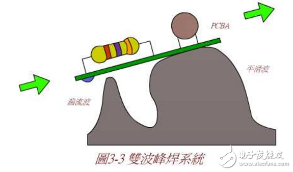
The soldering mechanism of the lead-free wave soldering is to form a molten solder of a specific shape on the liquid surface of the solder bath by the action of the power pump, and insert the components on the PCB and the conveyor belt through a certain angle and A certain immersion depth passes through the solder peaks to achieve solder joint welding.
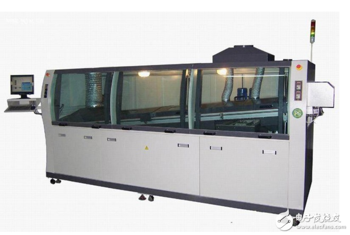
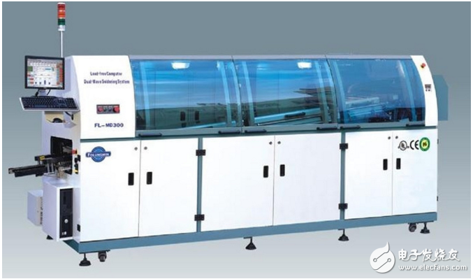
The new wave soldering machine that has just been manufactured is not divided into lead-free and lead-free. It is only differentiated when it is used. Generally, the lead-free wave soldering has a mark that is internationally common "pb" or lead-free mark. Leaded or lead-free wave soldering machines are not distinguishable in appearance (mainly using leaded tin or lead-free tin) mainly because the PCB produced contains lead. Lead-free wave soldering can directly produce leaded PCB. If lead is converted to lead-free again, the tin bath must be cleaned and replaced with lead-free tin.
Selection of multi-variety small batch production requirements;
The best fit for a variety of process technology requirements;
Easy to install, debug, maintain and maintain, reducing equipment maintenance costs;
Flexible selection of multi-level flux management system to meet environmental requirements;
The infrared and hot air heating modes can be combined arbitrarily to meet the production requirements;
Flexible selection of chillers and air-conditioners for easy and efficient flexible cooling.
Humanity and digital designProcess parameters, height and angle, guide rail width limit temperature digital display, through the quantitative setting, improve the precise control of process capability;
The whole module and module adopt high temperature glass visual design to improve the operability and monitorability of the equipment;
Built-in soldering defect help menu and equipment maintenance manual to enhance equipment added value.
Three new technologiesThe new anti-corrosion cast iron tin furnace effectively prevents the corrosion of the solder, and replaces it for 5 years to improve the service life and reliability of the equipment;
Low-oxidation device, effectively preventing "tofu residue", and controlling oxidation amount below 0.3KG/hour;
The patented design of spout, runner and impeller can control the smoothness of the peak within 0.5MM to improve the welding quality of the equipment.
Six major defects often found in lead-free wave solderingThe common welding defects and causes in lead-free wave soldering are as follows (only the defects that we often encounter in production, which we can see in real production). Of course, we must target specific defects in production. The phenomenon is judged and the appropriate solution is used to eliminate it.
1. LianxiThe main reason for the connection of tin is solder quality change, excessive impurities (generally copper exceeding the standard), poor solder quality or improper coating density, and short soldering time in the process, preheating or low solder temperature, resulting in baking solder It is impossible to sufficiently wet and spread in the weld zone to form excessive build-up, or the surface tension of the solder bump cannot overcome the cohesion of the solder rib and shrink to form a solder joint. Exhaust effects in mixing, shadowing effects, or too small pad spacing for small chip components are also important causes of bridging. The pin pitch of the components is too small (the load can not be small and 2MM), the component leads are too long will lead to the connection of tin, the PCB design is not reasonable, the design of the tin-free pad can not meet the requirements in the actual welding process. Lead to the tin. Therefore, waveform selection, transfer angle control, and PcB and component layout design in soldering are important.
2. TipThe reason for the sharpening is mainly due to the deterioration of the quality of the solder (heat transfer is not required), the solderability of the soldered end of the component is not good, and the process conditions are not good (such as the waveform is not good, the transmission angle is too small, If the transfer speed is too fast and the soldering time is too short, or the preheating temperature and the solder temperature are low, the molten solder cannot be shrunk into a well-shaped solder joint under the surface tension.
3. Virtual weldingThe main reason for the solder joint is the poor solderability of the solder joints, leads or pads of the components (such as poor plating or oxidation of the components), insufficient flux removal or poor coating quality, preheating temperature or thermal insulation. The time is insufficient and the flux action is not fully utilized. Solder quality changes are also a possible cause of solder joints. Unreasonable setting of process parameters (such as too fast speed, too high track, too high peak and tin furnace) are the main reasons for the solder joint. The solder joint does not form the necessary metallurgical connection with the soldered gold. The connection is not strong, but it will cause a false phase of circuit connection.
4. Tin thinThe main reason for tin is that the pad or metallized via is too large, the solder joint of the component is poor, the solderability of the solder is poor, or the solder coating is uneven. The solder contains insufficient tin and the solder temperature is too high, and the conveyor speed is too high. Such as the capillary action is not sufficient, the solder is not filled properly in the pad, and the filling amount is too small. The PCB manufacturing process is not rigorous enough, or the PCB is not in compliance with the standard, and the placement time is too long.
Leakage is caused by the fact that no solder joints are formed in the soldering area, which are caused by poor solderability of solder joints or leads, poor solderability of PcB local pads due to uneven solder coating, and insufficient flux activity. This causes the solder to fail to form a connection between the solder terminals and the leads and pads. Unstable running of the conveyor belt or unstable solder waves is also a possible cause.
6. Pcb deformationThe pcb deformation is mainly caused by unreasonable or faulty structure of the centering device on the conveyor belt, uneven preheating of the PCB or excessive preheating temperature, high welding temperature and long time. The deformation problem is also related to PCB material, component structure and assembly layout design. When the components are complex in structure and equipped with various types of components with large differences in heat capacity, special attention should be paid to the preheating control of the components to increase the uniformity of preheating. Multi-zone welding furnace heating can be considered. At the same time, the component layout design is optimized to control the thermal deformation of the PcB. When welding, strictly control the welding time and temperature to avoid the components staying in the high temperature environment for a long time. Excessive temperature or excessive wave soldering time may also damage the bonding of the PcB substrate to its upper pads and bars, causing it to peel and warp.
The main problems to be faced when conducting lead-free wave soldering are as follows:
The accumulation of tin slag is very unfavorable for lead-free peaks. If there is a deposit of tin slag in the tin bath, the tin slag may enter the peak. An inert gas can be used to prevent the dross from entering the peak.
Gloss is not very good: because of the presence of phosphorus, the gloss will not be very good, but it has no effect on the quality of the weld.
There are many problems with poor welding and need to be reduced: it has high performance requirements for the equipment, and also has requirements for welding time, contact surface and temperature. Generally, the board surface temperature should not exceed 140 °C. If the design is unreasonable and the temperature of the board is lowered, soldering defects will occur.
Solder Oxidation: When the solder is oxidized, black oxide powder will appear during the soldering process and it can be re-mixed with the solder, which affects the soldering strength and the soldering quality. Therefore, the solder should be prevented from being oxidized.
When using lead-free wave soldering, the most important thing is to control the height of the peaks, so put the PCB into the lead-free wave solder and apply solder to the solder joints. In order to keep the height of the lead-free wave soldering unchanged, a closed-loop control is added to the peak and the sensor is placed on the guide rail of the conveyor chain to facilitate the measurement of the height of the lead-free wave soldering while maintaining the immersion tin. The height is such that the speed of the tin pump drops rapidly.
Sfp Fiber Adapter,St Fiber Coupler,St Fiber To Ethernet Converter,Sfp To Sc Adapter
Ningbo Fengwei Communication Technology Co., Ltd , https://www.fengweicommunication.com