At present, the application of GNSS satellite navigation and positioning system is more and more extensive, including China, the United States, the European Union, Russia and other major powers in the world are actively deploying their own global satellite navigation and positioning system. Although China started late in satellite navigation, technology has developed rapidly. With the gradual improvement of China's Beidou-2 satellite navigation system, China has become the third country after the United States and Russia to have a complete navigation system. The demand for navigation receivers in the domestic market is also increasing. Designing high-performance, multi-mode, and low-cost navigation receivers has become a research hotspot. As an indispensable device in the development of navigation receivers, the acquisition and playback system has broad application prospects. Therefore, there is an urgent need to design a GNSS navigation signal acquisition and playback system with low price, good portability, intuitive interface and strong operability.
In summary, the monitoring end of the system uses an ARM processor based on the CortexA8 series. The processor takes into account both cost and performance requirements, and can design a beautiful graphical user interface. The system works at two frequency points of BD2-B1 and GPS-L1. It has good portability and intuitive interface. It can be operated by buttons or touch screen. At the same time, it can collect navigation satellite signals under complex outdoor environment at any time, which greatly improves Development efficiency and quality of navigation receivers.
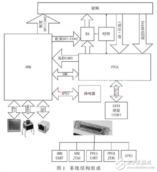
1 System structureThe system is divided into two parts: RF module and baseband module. Among them, the radio frequency module is responsible for receiving and sending radio frequency signals, and converting the radio frequency signals into baseband signals and then handing them over to the baseband module for processing; the baseband module completes functions such as user interaction and interface docking. In addition, it also includes SSD hard drives (data storage media, storing collected and playback data) and various external interfaces. The structural composition of the system is shown in Figure 1.
2.1 RF module
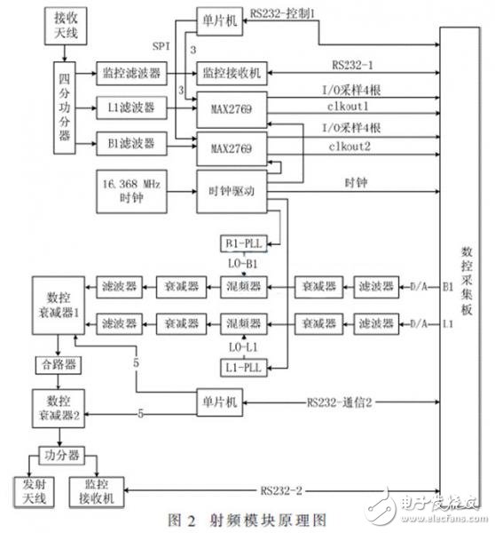
The RF module can be divided into two parts: up-conversion and down-conversion. The core device of the down-conversion part uses the MAX2769B chip. This chip is a multi-mode navigation receiver chip, which is suitable for GPS/Beidou/Glonas/Galileo satellite navigation. GPS. The gain control device of the up-conversion part adopts the HMC472LP4 numerical control attenuation chip. The attenuation chip is stepped by 0.5 dB and the maximum attenuation is 31.5 dB. They are respectively controlled by 6 pins V1~V6, and the low level is effective. The up and down conversion part is configured by C8051F230 single chip microcomputer. The down conversion part uses GPIO port analog SPI interface to write configuration words to the MAX2769B chip and configure related parameters. The up conversion module controls the level of the 12 GPIO ports to configure the gain. At the same time, the up-down conversion part of the radio frequency module adopts ATGM332D navigation receiver of Hangzhou Zhongke Microelectronics as the monitoring receiver. The up-down conversion module sends the message information received by the monitoring receiver to the FPGA module through the serial port, and the FPGA chooses to output to ARM side. Figure 2 is a schematic diagram of the RF module.
2.2 Baseband module
The baseband module can be divided into three parts: FPGA module, ARM module and baseband backplane. The baseband backplane is the bridge connecting each module and completes all functions except ARM and FPGA. Each module is connected to the backplane in the form of a connector. Here innovatively uses SSD hard disk for data storage to meet the large capacity space requirement of the device for collecting data for a long time. Due to the high complexity of the system, this article only introduces the design scheme of the power supply and clock circuit for the baseband backplane submodule.
2.2.1 FPGA module
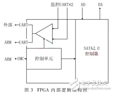
FPGA uses Xilinx's XC7K325TFFG900-2 FPGA (hereinafter referred to as K7). The K7 series is Xilinx's latest low-cost, high-performance FPGA for the low-end market. The K7 core board is mainly responsible for docking the RF data interface and high-speed transceiver interface. The internal logic structure of the FPGA is shown in Figure 3, which is roughly divided into three parts according to the function: control unit, SATA controller, UART distribution unit. The control unit of FPGA is mainly responsible for the error control of the system and the communication with the ARM end. Here ARM and FPGA communicate through the SMC bus, and the SMC bus driver of the K7 processor needs to be written in the Linux kernel.
2.2.2 ARM module
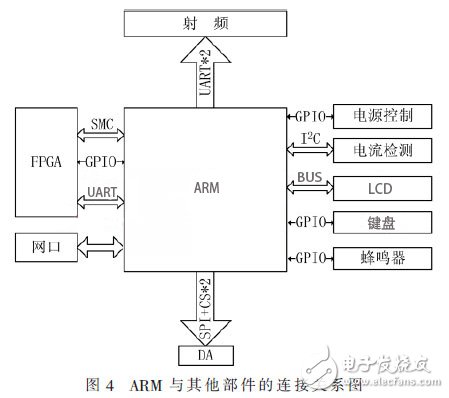
The ARM module uses Atmel SAMA5D31 processor, which is based on the Cortex-A5 architecture and has a main frequency of 528 MHz. It integrates a floating-point arithmetic unit and is a high-performance, low-power embedded processor. The ARM module integrates 256 MB ROM and 256 MB RAM to ensure performance while reducing development costs. For this system, the selection of this module is the result of considering various comprehensive factors such as performance, power consumption, and price. ARM as the main control chip to control the entire system flow, Figure 4 shows the connection relationship between ARM and other components.
2.2.3 Baseband backplane (power and clock)
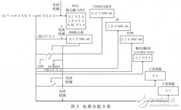
This design uses a 5 V ~ 42 V wide voltage power input. According to the current required by each device during operation, a 12 V/5 A adapter is used as the input power. The overall power distribution is shown in Figure 5.
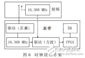
There are two clock sources for the entire system, both of which are active crystal oscillators of 16.368 MHz, which are located on the baseband backplane (master clock) and radio frequency board (standby clock). Normally, the main clock is used, and the backup clock is used in special applications. In addition to the 16.368 MHz clock, ARM has its own passive crystal oscillator as its own clock source. The module uses asynchronous communication mode to avoid errors caused by clock difference. Figure 6 shows the clock design of the system.
3.1 FPGA programming
When the system is collecting data, the FPGA receives the 8-bit AD digital signal (L1+B1) from the down-conversion module, after processing, it is stored in the SSD hard disk through the SATA interface to complete the data collection and storage; during playback, the FPGA The data is read from the SSD hard disk, after DA digital-to-analog conversion, it is sent to the up-conversion module to complete the signal broadcast. During satellite signal acquisition and playback, the FPGA should receive UART information from the up-down conversion module monitoring receiver to determine whether the collected and broadcast signals are normal.
This design uses VHDL language to describe the circuit that needs to be implemented. The number of high-speed transceivers (GTX) integrated in Xilinx's K7 series FPGAs is up to 16, and the speed of a single GTX can reach 12.5 Gb/s. GTX is the core of the SATA protocol. The device is more than enough to implement the SATA2.0 controller. This article uses K7 to realize the physical layer, link layer and transmission layer of the SATA protocol, mainly including the completion of link initialization, frame encapsulation, frame transmission/pause/end control, frame analysis and verification. The transmission layer of the SATA protocol is implemented by a Gigabit transceiver GTX, an OBB control module and an interface transmission rate selection module. The main functions of GTX include 16B/20B encoding/decoding, serial-parallel/parallel-serial conversion, comma detection, clock correction, prediction weighting, and linear equalization. The OBB control module is used for the power-on process of the hard disk or the reset process of the hardware, and at the same time establishes a communication link with the SATA controller.
3.2 ARM programming
As the core control module of this system, the ARM module is responsible for the scheduling of various tasks, plus the need for a friendly user interaction interface, so embedded Linux is used as the operating system of the ARM module. According to ARM tasks, it can be roughly divided into: user interaction, module instruction configuration, data file management, and module status monitoring.
First, you need to implement the driver for the corresponding interface in the Linux kernel. In addition to the SMC bus driver, Atmel officially provides the driver for other interfaces in the linux3.6.9 version of the kernel. You only need to draw the corresponding device in the device tree file. Node. Atmel officials also provide test programs for SPI, I2C, and GPIO interfaces. You can directly transplant the corresponding programs to Qt4 to implement the corresponding functions. What needs to be emphasized here is the UART interface. There is no specific class for serial communication in Qt4. This system refers to the third-party qextserialport class and customizes a PortSetTIngs type structure for storing serial port parameters. Since the Linux system does not support the serial port interrupt mode, it is necessary to create a new timer QTImer, timing 1 s, and synchronize the serial port transmission and reception in the program. Next, call the open() function to open the serial port, and call the bytesAvailable() function to determine whether the serial port data is zero. If there is data in the serial port buffer, call the readAll() function to read all the data in the buffer into the QByteArray type variable.
To achieve real-time receiver monitoring, it is necessary to analyze the message data received by the serial port, extract the carrier-to-noise ratio information, and draw a histogram for real-time display of signal quality. This system proposes a brand-new message parsing method for the Qt4 user graphical interface. First, we need to convert the QByteArray type variable to QString type, and call the replace() function to replace all the asterisks and carriage returns in the message with Comma, with comma as the delimiter, call split() function to split the message, find the $GPGSV field by query, and save the satellite number and carrier-to-noise ratio into the array. According to the data in the array, use a third-party QCustomPlot class to draw the histogram of the load-to-noise ratio. First call the setLabel function to set the horizontal and vertical coordinate names, and use the QCPBars provided by QCustomPlot to represent the histogram, and call the setData() function to perform each column. Assign, and then call addPlittable() function to add the histogram to the Widget. The horizontal coordinate assignment needs to call setTIckVector() and setTIckVectorLabels(), and finally call replot() to redraw the histogram to ensure that the histogram is updated in real time.
4 Experiment and verification
Because of the superiority of Qt4 in interface design, you can change the interface style at any time according to your needs.
In order to verify whether the serial port blocking phenomenon has occurred in the ARM-side program and whether it meets the real-time requirements, the processing time of each frame of packet is analyzed. Transplant the program to the embedded development platform, use labsat to replay a segment of the satellite's intermediate frequency signal, the intermediate frequency signal contains GPS and BD2 message information, after 3.5 hours of continuous testing to obtain a set of data, the data is analyzed by MATLAB To get the results shown in Figure 7.
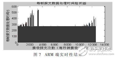
It can be clearly seen from Figure 7 that the message parsing and drawing time is mostly around 250 ms, and occasionally the burst time will reach a peak of 550 ms, and the processing time is within 1 s, which fully meets the real-time requirements.
5 ConclusionThe portable GNSS navigation signal acquisition and playback system designed in this paper realizes the storage and playback of satellite intermediate frequency data. Its monitoring terminal adopts the ARM processing platform, writes the SMC bus driver for K7 FPGA, and designs the corresponding graphical operation interface. While saving costs, it maintains good operability of the device, and uses SSD as a storage medium to ensure the device's long-term collection requirements. Here we use MATLAB to analyze the spectrum and power spectrum of the intermediate frequency signal, and we know that the quality of the playback signal meets the needs of the navigation receiver test. At the same time, the intermediate frequency data saved by it provides reliable original data for the research of signal acquisition and tracking algorithms. It laid the foundation for the development of high-performance, low-cost navigation receivers.
Video Brochure
 |
Video Brochure,LCD Video Booklets,MP4 Greeting cards as the Multimedia Promotional Plan, have been widely
used in some occasings, such as graduations, birthday parties, weddings, opening veremonies, company intruction
and other commercial or industrial purposes.
· High resolution LCD screens use thin-film transistor technology for the ultimate display
· Crystal clear audio that is synced with your video
· Custom designed, printed and programmed for UP remium mailable package for Video PrintAd
Specifications:
· LCD SCREENS: 2.4″, 2.8",3.5″, 4.3″,5", 7.0″,10.1"
· MEMORY: 256MB~2G (15 – 60 Minute Video Playback)
· LIFE: 2-3 hours of continuous playback, 6-12 months standby (battery life)
· USB PORT: Usb access for recharging unit and uploading/modifying content
· BATTERIES: Internal Li-ion battery. Rechargable via USB. 15-30mins recharge time.
Options:
· Buttons for Multiple Video Activation
· On/Off Button
· On-Open Activation via a Sensor
· Volume Control
· Specialty Finishing (Spot UV, Embossing, Gold/Silver Foil, Pantones, Metallic Inks, more)
· Cover Materials: Card Stock, Board stock, Leather & Plastic
· AC Power Source Capable
· Continuous Run Cycle
· Motion Activation
· USB Cable
Video Brochure, Video Brochure Card, LCD Video Brochure
AST Industry Co.,LTD , https://www.astsoundchip.com