Abstract : A PCI-I2S audio system based on FPGA is proposed. By combining PCI soft core, FIFO and designed interface circuit in FPGA, PCI, I2C, I2S and other buses are realized on FPGA, and audio data transmission and playback of different sampling frequencies are realized by combining audio decoder. Features. The system makes full use of the on-chip resources of the FPGA and its programmable features, reducing the complexity of the hardware circuit.
The I2S bus is a serial bus standard for transferring data between audio devices. The bus uses separate clock and data lines to avoid time-induced distortion. With the widespread use of multimedia, the bus has been used in more and more digital systems.
The PCI bus is a high-performance 32/64-bit local bus. The theoretical maximum transmission rate is 132 Mbit·s-1. It can support multiple sets of peripherals. It has been used as a bus label by various mainstream processors. It is currently applied. The widest range of peripheral buses. Most processors today do not have an integrated I2S interface, but in embedded systems, the CPU often uses the PCI bus to interact with peripheral devices. Therefore, a PCI-I2S interface conversion circuit needs to be designed to enable the CPU to communicate with peripheral audio devices. At present, the implementation of such an interface conversion circuit mainly realizes a PCI-based audio playback device by combining a dedicated interface chip such as a PCI interface chip and an audio interface chip in a board-level circuit. Although such a circuit is mature and reliable, the circuit design is complicated, the flexibility is small, and a large amount of board space is required.
With the development of digital communication technology, due to the flexibility of FPGA and its short development cycle, the application in interface circuit design has become more and more extensive. This paper proposes an interface conversion circuit that implements PIC-I2S using FPGA, which not only avoids the use of protocol conversion chip, but also saves space on the circuit board, and also greatly enhances the flexibility of the system and facilitates maintenance and upgrade.
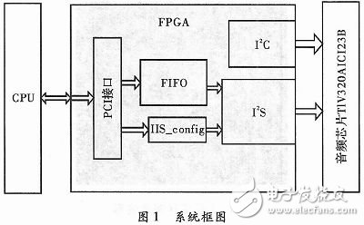
1 system hardware designThe audio playback system is mainly composed of stereo audio codec TLN320AIC23B, FPGA device XC6SLX75 and processor PowerPC8270. The system block diagram is shown in Figure 1. The CPU transmits the original audio data to the FPGA through the PCI bus and serially transmits it to the audio chip TLV320AIC23B in a 16-bit format for each group of data, and the digital chip converts the digital quantity into an analog audio signal output. FPGA implements PCI interface function and configuration and data transmission function of audio codec chip. Its internal is mainly composed of PCI protocol interface, I2S protocol interface, I2S configuration register, I2C protocol interface and FIFO memory.
TLV320AIC23B realizes the conversion of digital audio information to audio analog in the system. When the system is powered on, it first needs to configure its multiple control registers through the I2C interface. After that, the chip will control according to the bit transfer clock (Bclk) and left and right channels. The clock (LRCIN) captures the audio data sent by the FPGA as configured in the control registers. The received data will be transmitted to the chip for digital-to-analog conversion, filtering and other processing.
According to the I2S protocol specification and chip requirements, the FPGA generates a bit transfer clock (Bclk) and a left and right channel control clock (LRCIN) by the main clock (MCLK), and transmits it to the TLV320AIC23B synchronously with the audio data. The left and right channel control clock (LRCIN) should be the same frequency as the original sample level of the audio data, according to I. The protocol specification and chip data of S, its bit transfer clock (Bclk) and the chip's main clock (MCLK) are as follows:
BCLK=Sampling Size&TImes;Sampling Rate (1)
MCLK=Sampling Size&TImes;Sampling Rate&TImes;384 (2)
Where Sampling Rate is the original sample level frequency; SamplingSize is the sample size.
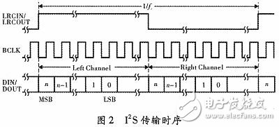
In the system, the TLV320AIC23B chip adopts the left-aligned interface mode, and its timing is shown in Figure 2. The left channel of the audio is strobed when LRCIN is high, and the right channel is strobed for low-time audio. The same set of data is transmitted on the left and right channels during one cycle of LRCIN. Since the transmission speed of the PCI bus is much higher than the transmission speed of the I2S bus, in order not to interrupt the response of the CPU too high frequency, a FIFO is generated in the FPGA, so that the PCI bus can continuously input a large amount of data. In addition, since different audio files have different sampling level frequencies, and usually the audio file is sampled at 16 kHz or 32 kHz, the I2S_config register is generated in the FPGA, which can be set via the PCI bus to call different numbers in the FPGA. Clock Management (DCM) to provide different clocks for the TLV320AIC23B chip.
The PCI protocol is more complicated. It not only has strict synchronization timing requirements, but also requires many configuration registers, so the implementation circuit is also complicated. Generally, there are usually three ways to implement a PCI interface in an FPGA: (1) designing a PCI interface by itself, which can selectively implement a PCI interface function as needed, which is closer to system requirements and can reduce system cost. However, developers need to have a deep understanding of the PCI protocol, and when the external environment is bad, it is not easy to meet the stability requirements of the system, and the development is difficult. (2) Using PCI hard core to develop the system, PCI hard core is the solidified circuit embedded in FPCA, similar to the dedicated PCI interface chip, the designer only needs to complete the signal link and verification, but in this method The PCI hard core has been solidified in the FPGA, which affects the flexibility of the system. (3) Using PCI soft core for development, the PCI soft core can be configured according to the user's own needs, more flexible, close to the user system, and it has been verified by the design manufacturer and has high reliability. This article uses the open source soft core MPCI32 provided by Mentor for the development of PCI interface on FPGA.
Molded Waterproofing Cable Assemblies
We specialize in waterproofing products overmolding. We can custom build, custom mold, and over-mold your cable designs.
We specialize in molded cable manufacturing for the widest diversity of
cable and connector types, across the whole spectrum of industries. Rich expeirence in developing and proposing solution Special for IP67, IP68 waterproofing products.
Molded waterproofing cable assemblies, waterproof wire harness, waterproofing cables overmolding
ETOP WIREHARNESS LIMITED , https://www.etopwireharness.com