Abstract: Based on the commonly used MEMS inertial device micro accelerometer, a design scheme using ARM and FPGA architecture to collect acceleration values ​​is introduced. The analog output signal of the micro accelerometer is processed and cached by the FPGA after being converted by the A/D chip. ARM receives the output data of the FPGA and displays and stores the data. How to use FPGA to realize the transmission control and data buffer of the data acquisition system, and the interface design of FPGA and A/D conversion chip and ARM, and realize the acquisition, transmission, display and storage of acceleration values. Flexible and versatile, it can be better transplanted into the data acquisition system of related devices.
0 Preface
An accelerometer is a widely used inertial sensor that can be used to measure the acceleration of a motion system. Most of the current accelerometers are micro-accelerometers designed and manufactured using micro-electromechanical technology (MEMS). Due to the adoption of micro-electromechanical technology, the design size is greatly reduced. A MEMS accelerometer has only a small part of the fingernail, and the MEMS accelerometer has Small size, light weight, low energy consumption and so on.
As micro accelerometers become more widely used, data signal acquisition and storage for micro accelerometers becomes extremely important. Most of the traditional data acquisition methods are completed by single-chip microcomputer. The programming is simple and flexible, but the shortcoming is that the control period is long and the speed is slow. Especially for the high-speed conversion data, the slow speed of the single-chip microcomputer greatly limits the data transmission speed. . The FPGA (Field Programmable Gate Array) has the advantage that the microcontroller can't match. The FPGA clock frequency is high, the internal delay is small, and all control logic is completed by hardware, which is fast and efficient, and is suitable for high-speed transmission control of large data volume. In high-speed data acquisition, FPGA has the advantage that single-chip microcomputer can't match. However, the interface of MCU is rich, and the data processing capability is strong, which is convenient for data display and storage operations.
Combining the advantages of MCU and FPGA, this paper introduces a micro-accelerometer data acquisition and storage system based on ARM and FPGA. It combines MXR6150G/M accelerometer sensor and TLC0820-A/D conversion chip to provide a flexible configuration and strong versatility. Data collection program.
1 system overall design
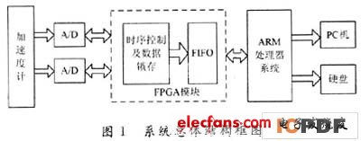
Figure 1 is a block diagram of the overall structure of the data acquisition system. The system is mainly composed of four parts: two-axis accelerometer, A/D converter, FPGA and ARM processor. The two-axis accelerometer outputs two analog signals, respectively representing the acceleration values ​​of the z-axis and the y-axis, and converts the input two analog signals into 8-bit digital signals through the A/D conversion chip, and the FPGA receives the A/D conversion chip. The digital signal is processed, and the processed data is processed by the ARM processor in an interrupt mode after being processed by the FIFO memory buffer in the FPGA. The collected data can be displayed on the PC in real time through serial communication, or through the serial communication. The IDE interface is stored to a large capacity hard drive.
2 system hardware design and implementation
2.1 MXR6150G/M accelerometer sensor
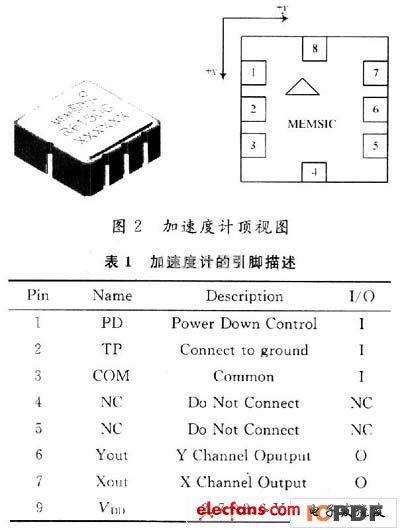
MXR6150G/M is a two-axis accelerometer sensor manufactured by Wuxi Meixin Semiconductor Co., Ltd. It is manufactured in a standard sub-micron CMOS process and can measure acceleration signals from -5g to +5g (g is gravitational acceleration). The two analog voltages are used to reflect the magnitude of the acceleration. When the accelerometer is stationary, the output voltage is 1.50 V and the voltage output sensitivity is 150 mV/g. Figure 2 is a top view of the appearance of the accelerometer. Table 1 shows the pin descriptions of the accelerometer, with pins 7 and 6 outputting the acceleration components of the x and y axes, respectively. The value of the actual acceleration needs to be combined with the values ​​of the x-axis and y-axis acceleration, which can be done by parallel computation processing of the FPGA.
2.2 8-bit A/D converter chip TLC0820
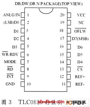
The TLC0820 is an A/D converter manufactured by Texas Instruments Inc. (TI) using an advanced LinCMOS process. It consists of two 4-bit flash (FLASH) converters, a 4-bit digital-to-analog converter, and a calculation. The error amplifier, the control logic circuit and the resulting latch circuit are composed. It uses 8-bit parallel output and does not require external clock and oscillating components. It is widely used in high-speed data acquisition systems, industrial control and factory automation systems. Its package leads are shown in Figure 3. The pin functions are described as follows: ANLG IN is analog input; chip select, low active; DO~D3, D4~D7 are tri-state data output; for interrupt output, indicating conversion end; MODE is mode selection input; ; for reading the input terminal; REF- is the reference voltage lower limit; REF+ is the reference voltage upper limit; VCC is the power supply voltage; is the write input/read status output.
2.3 Altera-FPGA and ARM Processor
The system's FPGA is implemented in Altera FPGA's Cyclone II family of EP2C35. The EP2C35 provides up to 33,216 logic elements (LEs), 35 18&TImes, 18-bit multipliers, 483 840b internal RAM blocks, and dedicated external memory interface circuits. Four phase-locked loops (PLLs) and high-speed differential I/O.
The ARM processor used in the system is Philips' LPC2210, based on a 16/32-bit ARM7TDMI-S CPU that supports real-time emulation and embedded tracking. The LPC2210's 144-pin package, extremely low power consumption, two 32-bit timers, eight 10-bit ADCs, PWM outputs, and up to nine external interrupts make it ideal for industrial control, medical systems, access control, and electronic receipts. Machine and so on. By configuration, the LPC2210 provides up to 76 GPIOs. Thanks to its built-in wide range of serial communication interfaces, it is also well suited for communication gateways, protocol converters, and many other types of applications.
Galvanized Steel Wire,Stay Wire,Guy Wire,Earth Wire
HENAN QIFAN ELECTRIC CO., LTD. , https://www.hnqifancable.com