There are many different types of analog-to-digital converters (ADCs), and it is always difficult to figure out which ADC is best for a given application. Data sheets tend to complicate matters, and many technical indicators affect performance in unpredictable ways.
When choosing a converter, engineers typically focus only on resolution, signal-to-noise ratio (SNR), or harmonics. Although these are important, other technical indicators are equally important.
Resolution, which is probably the most misunderstood technical indicator, represents the number of output bits, but does not provide performance data. Some data sheets list the effective number of bits (ENOB), which uses actual SNR measurements to calculate the converter's effectiveness. A more useful converter performance metric is the noise spectral density (NSD) in dBm/Hz or HznV. NSD can be calculated from known sampling rates, input ranges, SNR, and input impedance (dBm/Hz). Knowing these parameters, you can choose a converter to match the analog performance of the front-end circuit. This method of selecting an ADC is more efficient than just listing the resolution.
Many users also consider spurious and harmonic performance, which are independent of resolution, but converter designers typically adjust their design to match harmonics to resolution.
Power Supply Rejection (PSR) measures how the power supply ripple is coupled to the ADC input and appears on its digital output. If the PSR is limited, the noise on the power line will only be suppressed by 30 to 50 dB relative to the input level.
In general, unwanted signals on the power supply are related to the input range of the converter. For example, if the noise on the power supply is 20 mV rms and the converter input range is 0.7 Vrms, the noise on the input is -31 dBFS. If the converter's PSR is 30 dB, the coherent noise will appear as a -61 dBFS line in the output. PSR is especially useful in determining how much filtering and decoupling a power supply will require. PSR is very important in noisy environments such as medical or industrial applications.
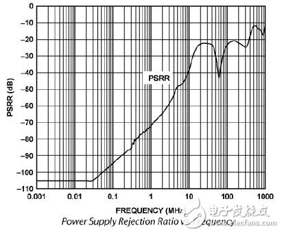
figure 1
Common mode rejection (CMR) measures the differential mode signal caused by the presence of a common mode signal. Many ADCs use differential inputs to achieve high immunity to common-mode signals because the differential input structure itself suppresses even-order distortion products.
Like PSR, power supply ripple, high-power signals generated on the ground plane, RF leakage from mixers and RF filters, and applications that generate high electric and magnetic fields introduce common-mode signals, although many converters do not specify CMR. But they usually have a CMR of 50 to 80 dB.
Clock-related technical indicators, although important, are not always specified and may be difficult to determine.
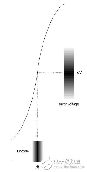
Figure 2. Relationship between input clock and sample noise
The clock slew rate is the minimum slew rate required to achieve rated performance. Most converters have enough gain on the clock buffer to ensure that the sampling instant is well defined, but if the slew rate is too low, the sampling instant is very uncertain and excessive noise will be generated. If a minimum input slew rate is specified, the user should meet this requirement to ensure rated noise performance.
Aperture jitter is the internal clock uncertainty of the ADC. The noise performance of the ADC is limited by internal and external clock jitter.
In a typical data sheet, the aperture jitter is limited to the converter. The external aperture jitter is added to the internal aperture jitter in a rms mode. For low frequency applications, jitter may not be important, but as the analog frequency increases, the noise problem caused by jitter becomes more apparent. If you don't use a sufficient clock, performance will be worse than expected.
In addition to the increased noise due to clock jitter, spectral lines in the clock signal that are not harmonically related to the clock will also appear as distortion of the digitized output. Therefore, the clock signal should have as high a spectral purity as possible.
The aperture delay is the time delay between the application of the sampled signal and the moment when the input signal is actually sampled. This time is usually nanoseconds or less and may be positive, negative or even zero. The aperture delay is not important unless it is important to know the exact sampling instant.
Conversion time and conversion delay are two closely related technical indicators. The conversion time is generally applicable to successive approximation converters (SARs), which use a high clock rate to process the input signal. The input signal appears on the output for a significantly longer time than the conversion command, but before the next conversion command. The time between the conversion command and the completion of the conversion is called the conversion time.
Conversion delays are typically applied to pipelined converters. As a specification for measuring the number of pipelines (internal digital stages) used to generate digital outputs, the conversion delay is typically specified by pipeline delay. The actual conversion time can be calculated by multiplying this number by the sampling period used in the application.
Wake-up time, in order to reduce the power consumption of power-sensitive applications, the device is usually turned off during periods of relative use. This does save a lot of power, but when the device restarts, the internal reference is stable and the internal clock is functionally restored. It takes a certain amount of time, and the converted data will not meet the technical indicators.
Output load, like all digital output devices, ADCs, especially CMOS output devices, specify output drive capability. For reliability reasons, knowing the output drive capability is important, but the best performance is generally when the full drive capability is not reached.
In high-performance applications, it is important to minimize output load and provide proper decoupling and optimized layout to minimize voltage drop across the supply. To avoid this type of problem, many converters provide LVDS output. LVDS is symmetrical, thus reducing switching current and improving overall performance. If you can, you should use the LVDS output to ensure optimal performance.
A standard is not specified and a critical unspecified project is the PCB layout. Although there are not many things that can be specified, it can significantly affect the performance of the converter. For example, if the application fails to use sufficient decoupling capacitors, there will be excessive power supply noise. Due to the limited PSR, noise on the power supply can couple into the analog input and destroy the digital output spectrum, as shown in Figure 3.
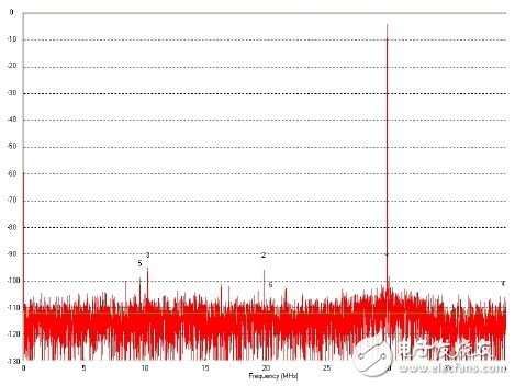
Figure 3a
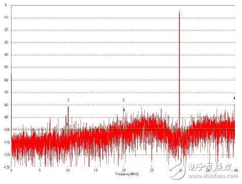
Figure 3b
Magic 5 Inch LED Downlights can be detachable in two parts. One 12W/15W module, and 4 Inch size rings.
1. 5 Inch LED Downlights long life up to 25000Hrs.
2. 5 Inch Led Downlights can save 80% energy
3. Color temperature of 5 Inch LED Downlights: warm white, nature white, cool white.
4. Rate voltage of 5 Inch LED Downlights: AC100-240V.
5. Frequency of 5 Inch LED Downlights: 50HZ.
6. 5 Inch LED Downlights with 2 years Warranty.
7. Dimmable & CCT Changeable Downlight can be abvailable.
8. White, black, silver corlor for option.


5 Inch LED Downlights
5 Inch LED Downlights,5 Inch Square LED Downlights,5 Inch Dimmable LED Downlights,Recessed LED Downlight
SHENZHEN KEHEI LIGHTING TECHNOLOGY CO.LTD , https://www.keheiled.com