First, the design features
1, constant current output is very suitable for driving LED
2. The high output voltage supports one LED string, so there is no need to consider the current distribution between the LEDs.
3. Provide protection against load disconnection, short circuit and overheating
4. High efficiency over the entire operating voltage range (>80%)
5, small and lightweight, low cost, few components of the design
6, no transformer required - use a simple single inductor
7, in line with EN55022B conducted EMI limits
Second, the circuit schematic
Figure 1. Circuit diagram of a 554 V 11W constant current boost converter for driving an LED array
Third, the working principle analysis
The power supply shown in Figure 1 uses a LinkSwitch-TN device in a boost converter configuration that provides a constant current of 20 mA from a single positive voltage of 554 VDC (referenced to the neutral input voltage). This power supply provides an ideal drive solution for a single LED string.
The fusible resistor RF1 not only provides protection against severe faults, it also limits the inrush current generated during the first power up. Diode D1 is used to provide half-wave rectification of the input AC voltage. Capacitors C2, C3 and inductor L2 form a π-type filter circuit that reduces conducted EMI.
After LNK306 (U1) is turned on, the current flowing through the input section (consisting of U1 and boost inductor L1) will gradually increase. The voltage across inductor L1 is equal to the rectified and filtered voltage on C3 (Vin). At this time, a gradual increase in current will cause energy to be stored in the inductor L1.
After U1 is turned off, in order to maintain the same inductor current, the polarity of L1 will be reversed, D2 will be forward biased, and current will flow into C1 and the load. After U1 is turned off, the voltage on L1 is the voltage difference between the output voltage and the input voltage. It can be seen from the figure below that this voltage is in series with the input voltage (on C3), so this configuration can gradually increase the input voltage (boost).
The boost diode D2 is a high voltage ultrafast recovery diode. C1 acts as an output filter capacitor. VR1, VR2, and VR3 are used to control the output voltage to 600 V in the event of a load disconnect or open loop fault. Capacitor C5 and resistor R2 form an RC buffer snubber circuit that reduces conducted EMI caused by switching during D2.
Inductor L1 is the boost inductor, and its minimum value can be calculated by the following formula:
Among them, Po is the output power, ILIM is the minimum current limit, and FS(MIN) is the minimum switching frequency of U1. This design uses a standard 2200μH inductor available from stock.
Resistor R1 acts as a current sense resistor and the resulting voltage is sensed in real time by the FB pin. The output regulation is maintained by a switch control circuit that enables and disables (skips) the switching cycle based on voltage changes and load conditions. The feedback (FB) pin of U1 is sampled at the beginning of each conduction cycle. If the current flowing into the FB pin exceeds 49μA, the current cycle will be skipped.
Fourth, design points
Diode D2 uses an ultrafast recovery diode with a reverse recovery time (tRR) of 75 ns or less and a reverse peak rated voltage that exceeds VOUT. In order to reduce the D2 reverse recovery current spike generated when U1 is turned on, the design operates in discontinuous conduction mode.
The fusible resistor RF1 should be a wound-type flame retardant resistor to protect the circuit in the event of current surges and differential mode surges.
By using AC input full-wave rectification, the values ​​of capacitors C2 and C3 can be greatly reduced. Capacitor C4 is the bypass capacitor for U1 and should be placed close to its source and BP pins.
The output capacitor C1 is selected according to the output ripple current requirement. If VRIPPLE is the desired ripple voltage, the output capacitor can be calculated by the following formula:
Among them, the maximum value of the Lmax inductor (the tolerance coefficient of the inductor), the maximum current limit of I lim, and Vout is the output voltage.
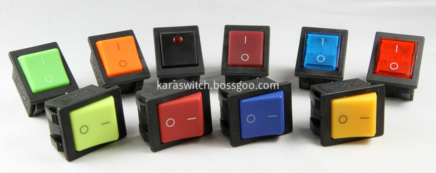
The range of switch models comply with UL 61058-1 and CAN/CSA-22.2 No61058-1-05,for the United States and Canada.This series items are all high quality,and sale good.Many colors can be met.Especially,model KR2-11has high ampere,used wildly in the industrial area.
One of them,item KR2-11-201D is our hot sale item:

UL Approved Switch,New UL Approved Switch,UL Approved Micro Switch
Ningbo Kara Electronic Co.,Ltd. , https://www.kara-switch.com