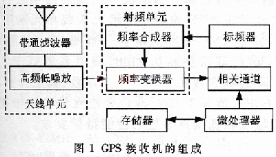
When GPS satellites are used for navigation and positioning, the main task of the user receiver is to extract the pseudorandom noise code and data code in the satellite signal to further calculate the navigation information such as the position, velocity and time (PVT) of the receiver carrier. Therefore, GPS receivers are vital user equipment. At present, the practical application of the GPS receiver circuit generally consists of four parts: an antenna unit, a radio frequency unit, a communication unit, and a resolving unit, as shown in FIG. Based on the analysis of GPS satellite signal composition, the principle and application of RF front-end GP2010 are given.
This article refers to the address: http://
1 Composition of GPS satellite signals
GPS satellite signals are synthesized using a typical code division multiple access (CDMA) modulation technique (as shown in Figure 2). The complete signal mainly includes three components: carrier, pseudo-random code and data code. The signal carrier is in the L-band, and the center frequencies of the two carriers are denoted as L1 and L2, respectively. The satellite signal reference clock frequency f0 is 10.23 MHz, and the center frequency of the signal carrier L1 is 154 times the frequency of f0, that is:
fL1=154×f0=1575.42MHz (1)
Its wavelength λ1 = 19.03 cm; the center frequency of the signal carrier L2 is 120 times the frequency of f0, namely:
fL2=120×f0=1227.60MHz (2)
Its wavelength λ2 = 24.42 cm. The frequency difference between the two carriers is 347.82 MHz, which is about 28.3% of L2. Thus, selecting the carrier frequency is convenient for measuring or eliminating the propagation delay error caused by the ionospheric effect when the navigation signal propagates from the GPS satellite to the receiver. The pseudo random noise code (PRN), that is, the ranging code mainly has two types: fine ranging code (P code) and coarse ranging code (C/A code). The code rate of the P code is 10.23 MHz, and the code rate of the C/A code is 1.023 MHz. The data code is navigation positioning data that is transmitted by the GPS satellite to the user receiver in binary form, also called navigation message or D code. It mainly includes satellite calendar, satellite clock correction, ionospheric delay correction, working state information, C/A code conversion. To capture the P code information and the summary ephemeris of all satellites; the total message consists of 1500 bits, divided into 5 sub-frames, each sub-frame transmits 10 words in 6s, each word 30 bits, a total of 300 bits, so the data The code has a baud rate of 50 bps.
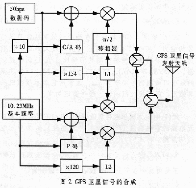
The data code and the two pseudo-random codes are respectively modulated on the L1 carrier in the in-phase and quadrature manners, and the P-code is used for the bi-phase modulation on the L2 carrier. Therefore, the complete satellite signals of L1 and L2 are:
SL1(t)=AcCi(t)Di(t)sin(ωL1t+φc) (3)
+ApPi(t)Di(t)cos(ωL1t+φP1)
SL2(t)=BpPi(t)Di(t)cos(ωL2t+φp2) (4)
Where, Ap, Bp, and Ac are the amplitudes of the P code and the C/A code, respectively; Pi(t) and Ci(t) are the pseudo-random sequence codes corresponding to the P code and the C/A code, respectively; Di(t) is The satellite navigation message data code; ωL1, ωL2 are the angular frequencies of the L1 and L2 carrier signals, respectively; φC and φP1, φP2 are respectively the C/A code and the P code corresponding to the initial phase of the carrier. The synthesized GPS signal is transmitted to the world, and is used by the receiver to solve the navigation and positioning information anytime and anywhere.
2 GPS receiver sensitivity
The quality of the GPS receiver's detection depends on the signal-to-noise ratio. When it is an “ideal receiverâ€, the signal-to-noise ratio Si/Ni at the receiver input is the same as the signal-to-noise ratio So/No at its output. Due to the internal noise of the actual GPS receiver, (So/No)<(Si/Ni); and the larger the noise, the smaller the output signal-to-noise ratio, the worse the performance of the receiver, and the noise figure of the receiver at this time. for:
F=(Si/Ni)/(So/No) (5)
Equation (5) shows the multiple of the signal-to-noise ratio of the receiver output relative to the signal-to-noise ratio of the input terminal due to the influence of internal noise. From equation (5), the rated power of the input signal can be expressed as:
Si=NiFo(So/No) (6)
Equation (6) gives the GPS receiver's ability to receive satellite signals in the noise background. The receiver must not only amplify the output signal to a sufficient value, but more importantly, the signal-to-noise ratio So/No at the output must be achieved. ratio. Let (So/No) ≥ (So / No) min the minimum detectable signal power of the corresponding receiver input signal power is Simin, which is usually used to indicate the sensitivity of the receiver. Due to the receiver's input noise rating
Ni=kT0Bn (7)
In the formula (7), k is a Boltzmann constant, k=1.38×10 -23 J/K, T0 is an indoor temperature of the unit circuit of 17° C. (290 K, absolute temperature), and Bn is a bandwidth of the unit circuit. Substituting equation (7) into equation (6) yields:
Si=kT0BnFo(So/No) (8)
Therefore, the sensitivity of the GPS receiver can be further obtained as follows:
Simin=kT0BnFo(So/No)min (9)
It can be known from equation (9) that in order to improve the sensitivity of the GPS receiver, it is necessary to reduce the minimum detectable signal power Simin. Therefore, in the design of the receiver circuit, it is necessary to consider reducing the total noise figure Fo of the receiver as much as possible. Try to improve the signal-to-noise ratio So/No at the output of the GPS receiver in the noise background.
3 GPS receiver antenna unit
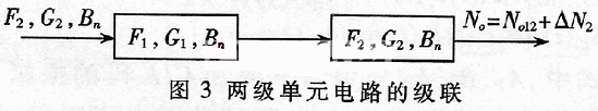
The main function of the antenna unit is to receive the airborne GPS satellite signals to provide a purer complete satellite signal for the receiver RF front end. In the receiver design, when two unit circuits are cascaded (as shown in Figure 3), if the noise figure and rated power gain of the first and second unit circuits are F1, F2, and G1, G2, respectively, the bandwidth is For Bn; if the total noise figure of the cascade circuit is Fo, then the rated noise function No of its actual output is:
No=kT0BnG1G2Fo (10)
Since No consists of two parts, namely:
No=No12+ΔN2 (11)
Where No12 is the rated noise power presented by the noise of the first-stage unit circuit at the output of the second-stage unit circuit, and ΔN2 is the noise power generated by the second-stage unit circuit, and
No12=kToBnG1G2F1 (12)
ΔN2=kToBnG2(F2-1) (13)
Substituting equations (12) and (13) into equation (11),
No=kToBnC1C2Fo
=kToBnG1G2F1+kToBnG2(F2-1) (14)
Simplify (14), the total noise figure after cascading two-level unit circuits is:
Fo=F1+(F2-1)/G1 (15)
Similarly, the total noise figure when cascading n-level unit circuits is:
Fo=F1+(F2-1)/G1+(F3-1)/(G1G2)+Λ+(Fn-1)/(G1G2ΛGn-1) (16)
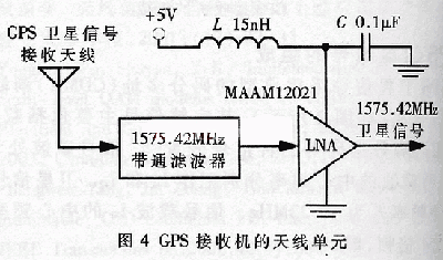
It can be seen that the internal noise of each unit circuit in the GPS receiver has different response to the total noise figure after cascading, and the noise coefficient of the unit circuit with the higher the number of stages has greater influence on the total noise figure. Therefore, the total noise figure mainly depends on the noise figure of the first few stages of the unit circuit, wherein the antenna thermal noise has the greatest influence on the receiver performance, so the design uses the receiving antenna, the RF band selection bandpass filter and the high frequency low noise amplifier ( Devices such as LNA) form an antenna unit (as shown in Figure 4). The antenna unit is powered by DC 5V. The LNA uses a high-gain, low-noise, high-frequency amplifier MAAM12021 with a gain of up to 21dB and a noise figure of less than 1.55dB, which is beneficial to reduce the total noise figure of the GPS receiver; its working frequency range is 1.5~ 1.6GHz, suitable for the frequency band requirements of C/A code GPS receivers, can meet the performance requirements of high gain and low noise figure.
4 GPS receiver RF unit
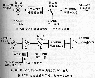
The noise bus is accompanied by signals at the same time. It is an important measure to improve the receiver sensitivity by increasing the signal-to-noise ratio at the output of the noise background. The frequency of the signal received by the GPS receiver antenna unit and supplied to the radio frequency unit is very high and the channel bandwidth is very narrow. To filter out the required channel directly, a filter with a very large Q value is required, at least the current technical level is difficult to satisfy. Indicators; In addition to the problems of gain, accuracy and stability of high-frequency circuits, it is unrealistic to directly demodulate GPS satellite signals in the high-frequency range. To this end, the circuit structure of the "superheterodyne" multi-stage frequency conversion matching zone filter is adopted in the design of the radio frequency unit to eliminate noise interference and solve the difficulties encountered in high-frequency signal processing. The chip suitable for this circuit structure uses the second generation GPS receiver RF front end GP2010. It is available in a 44-pin, frame-square package that integrates a frequency synthesizer, mixer, automatic gain control (AGC) circuitry, and digital quantizer. The signal frequency received by the GP2010 is compatible with the satellite signal frequency of the L1 carrier, and is mainly used to design the RF unit of the C/A code GPS receiver. The weak GPS high-frequency signal passes through the super-heterodyne three-stage mixing circuit, removes other channel interferences, obtains sufficient gain, demodulates and extracts the required intermediate frequency information. Figure 5 shows the working principle of the first two superheterodyne downconverters and the third stage mixer with automatic gain control (AGC) circuit. The frequency of the output signal decreases and amplitude after each down conversion. Increase, while interference from other channels and bands is gradually filtered out.
GP2010 uses a mixer to move the high-frequency GPS signal to a very low IF frequency while introducing image interference, and the effect of suppressing the image interference by the filter depends on the distance between the image frequency and the signal frequency, or It depends on the frequency of the IF frequency. If the IF frequency is high, the signal is far away from the image frequency, then the image frequency component can be greatly suppressed; conversely, if the IF frequency is lower, the signal is not far from the image frequency, and the filtering effect of the filter on the interference is Relatively poor. Since the channel selection is performed at the intermediate frequency, similarly, the higher intermediate frequency has higher requirements on the channel selection filter, so the image rejection and the channel selection form a contradiction, and the selection of the intermediate frequency becomes the key to the contradiction. . So in GPS receiver design, two or three frequency conversions are often used to achieve a better compromise.
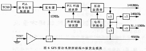
As can be seen from Figure 5, the GP2010's three-stage inverter uses three IF filters with center frequencies of 175.42 MHz, 35.42 MHz, and 4.309 MHz, respectively. The local oscillator signals required by the mixers at each stage are provided by an on-chip integrated phase-locked loop (PLL) frequency synthesizer (see Figure 6). It consists primarily of components such as a PLL oscillator loop, a phase detector, a PLL loop filter, a divider, and a complete 1400MHz voltage-controlled oscillator (VCO). The PLL uses a 10.000MHz reference frequency; the VCO has a control gain of 150MHz/V and an output frequency range of 1386 to 1414MHz. In order to provide a high stability reference frequency source, a temperature compensated crystal oscillator (TCXO) is used in the design to provide a 10.000MHz AC small signal frequency to the PLL oscillator from a reference frequency of 5kΩ. When the PLL phase locks the reference signal, the phase detection output logic high indicates that the phase is locked, the phase lock time is about 6ms, and the loop gain is about 150dB. The 1400MHz signal output by the VCO is used as the first local oscillation signal, and the 140.0MHz and 31.111MHz signals generated by the frequency division are respectively used as the second local oscillation signal of the second local oscillation. When the GP2010 receives the 1575.42MHz GPS satellite signal, the intermediate frequency signal of 4.309MHz can be obtained by the three-stage frequency conversion.
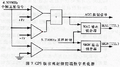
In order to cooperate with the channel unit and the solving unit to complete the data extraction and signal processing of the navigation signal, under the control of the 5.714MHz sampling clock, the GP2010 integrated digital quantizer can realize the digital quantization of the 4.309MHz IF satellite signal, thus the channel unit. The correlator provides a 2-bit quantized output of TTL level, ie 1.405 MHz binary symbol and magnitude digital information, as shown in Figure 7. In order to obtain a smooth IF satellite signal and sampled digital output, the module simultaneously generates an AGC control signal for stabilizing the amplitude of the IF signal generated by the third-stage conversion (as shown in Figure 5(b)).
In short, the GP2000 chipset is a series of integrated circuits introduced by Zarlink Semiconductor for the design of GPS receivers. The GP2000 chipset can be used to design multi-channel satellite signal receiving equipment. In the design of GPS receiver, the design of the antenna unit focuses on the influence of frequency band selection and high frequency and low noise on the total noise figure of the receiver to improve the sensitivity of the receiver. The RF unit uses frequency synthesis, frequency conversion, automatic gain control and other technologies. By relying on high-quality IF frequency selection, image rejection and channel selection filter, the received GPS signal is subjected to a series of processing such as frequency conversion, amplification, filtering, sampling, etc., thereby obtaining a digital intermediate frequency satellite signal. The well-designed superheterodyne GPS receiver can achieve high receiving sensitivity, frequency selectivity and large dynamic range, and has the advantages of simple structure, small size, light weight, and low power consumption.
Our latest USB Type-C socket offers optional splash protection (IPX4 level) and valuable circuit board design space.
Our latest USB Type-C socket protects equipment in harsh environments. It has the industry-leading IPX8 waterproof performance and meets the IEC60529 standard.
Waterproof USB Connector
ShenZhen Antenk Electronics Co,Ltd , https://www.antenk.com