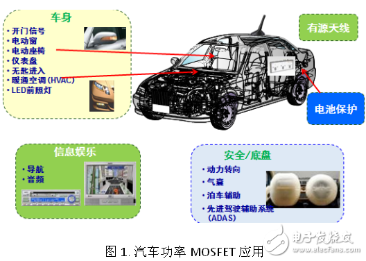
With the increasing trend of electronic functions of automobiles, more and more electronic components in automobiles, and increasingly harsh application environments, automotive design engineers need to consider various factors such as space and performance. Power MOSFETs provide low power consumption and smaller. Ideal size for a wide range of automotive applications, such as anti-lock brake system (ABS) hydraulic valve control, motor control for electric windows and LED lighting, airbags, HVAC systems, total power Applications, electronic power steering and infotainment systems, etc.
To advance MOSFETs for greater energy efficiency, ON Semiconductor has developed Fine pitch trench technology, clip bonding technology and the industry's leading ATPAK packaging technology. Micro-pitch trench technology provides lower on-resistance by reducing gate cell pitch, providing higher cell density and microstructure to improve energy efficiency and reduce power consumption. The pinch-welding technology greatly increases the current handling capability and provides a thermal path that directly extracts heat from the top of the die. The ATPAK package not only increases power density, but also improves current handling and heat dissipation.
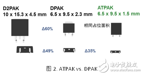
ATPAK package reduces size and increases power density
Fuel-powered vehicles and electric vehicles require smaller size and higher power density power devices. ON Semiconductor's unique ATPAK packaging technology meets this requirement. As shown in the figure below, the package size of ATPAK is greatly reduced compared to the traditional DPAK and D2PAK packages: DPAK is 60% smaller than the D2PAK footprint and 49% smaller, while ATPAK maintains the same footprint as DPAK. But the thickness has been reduced by 35%.
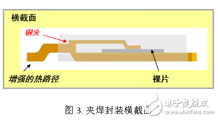
ATPAK package uses clip welding technology to improve heat dissipation
As the package size gets smaller, the temperature inside the device tends to increase because it becomes more difficult to derive excess heat. Heat dissipation is critical to total energy efficiency, safety, and system reliability. The ATPAK package uses clip-on soldering technology to minimize thermal impedance and total on-resistance, which greatly improves current handling compared to conventional metal wire bonded DPAK packages. Thermal impedance is the temperature rise caused by 1 W of heat, in °C/W. The lower the thermal impedance, the better the heat dissipation. Tests and comparisons were made using the same specifications of ATPAK and DPAK devices. The results show that the thermal impedance of the APAAK is 6 °C/W lower than that of the DPAK after the heat sink is used, even though the thermal impedance is the same even without the heat sink.
Conventional wire bonding uses gold, copper or aluminum to connect each electrode of a silicon chip in a package. However, since each line is relatively thin, this fundamentally limits current handling. This limitation can be reduced by adding more parallel wires, but this will affect the overall cost and there are practical limits on the number of wires that can be federally set. Since automotive power MOSFETs perform high current drive control in high temperature environments, low on-resistance is a key performance factor for automotive solutions. For MOSFETs with low on-resistance, the wire resistance can represent a fairly large total impedance in the package. Especially in applications where the on-resistance is required to be less than 20 mΩ, the impedance of the wire cannot be ignored.
The pinch-welding technology uses a copper clip to directly connect each electrode, which greatly reduces the electrical impedance of the drain-source path, thereby reducing the on-resistance and achieving better heat transfer. Test results show that the pinch bond reduces the on-resistance by 30% compared to the aluminum wire bond and reduces the on-resistance by 90% compared to the gold wire bond. Moreover, the pinch welding technology uses a copper plate with a wide cross-sectional area, which greatly improves the current handling capability and eliminates the problem of high current fusible wires in the conventional process.
ATPAK current handling capability is up to 100 A, which is the maximum current handling capability that D2PAK can achieve. Moreover, the cost of ATPAK is almost the same as that of DPAK. Therefore, the use of ATPAK instead of D2PAK in the design can reduce the package size by 50% and achieve the same performance, achieving the dual purpose of saving space and improving power processing capability without increasing cost.
Advantages of ATPAK P-Channel Power MOSFETs
Compared to competitors' P-channel MOSFETs, ON Semiconductor's ATPAK P-channel MOSFETs offer smaller size, lower on-resistance, higher current handling and better avalanche resistance. Avalanche resistance refers to the degree of vulnerability of the energy stored in the inductor to the power MOSFET. In addition, electrostatic discharge (ESD) is always a challenge to be overcome in packaging and practical use. ESD may occur in automotive applications due to mechanical friction. In addition, dry air tends to increase electrostatic discharge. ESD can cause mechanical failure. So ON Semiconductor's ATPAK P-channel power MOSFETs are embedded with protection diodes to enhance ESD robustness.
A charge pump is required to reduce the on-resistance compared to an N-channel MOSFET. The P-channel scheme eliminates the need for a charge pump and provides a simpler and more reliable drive with fewer components.
ON Semiconductor's P-Channel Automotive MOSFET Lineup
ON Semiconductor offers a broad portfolio of P-channel MOSFETs to meet a wide range of automotive applications. P-channel MOSFETs in the ATPAK package can be used in applications up to 65 W due to low on-resistance and excellent heat dissipation. Designers can choose the right MOSFET for their specific design needs.
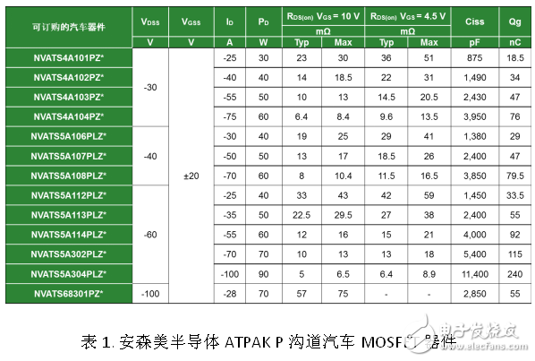
For example, the P-channel MOSFET NVATS5A108PLZ or NVATS5A304PLZ is used for reverse battery protection of automotive LED headlamps, which reduces conduction losses, simplifies circuits, and optimizes performance and component count.
to sum up
The continuous enhancement of the electronic function of automotive functions has made the automotive application environment increasingly demanding. The standard for improving system reliability and the requirement to reduce the component size to reduce the weight of the vehicle are becoming more important factors in the power device market. ON Semiconductor's innovative ATPAK package not only makes power MOSFETs slimmer, but also uses clip-on soldering technology to achieve up to 100 A of current handling capability, excellent heat dissipation for safety and reliability, and cost Equivalent to DPAK, the company offers a wide range of ATPAK P-channel power MOSFETs to meet a wide range of automotive applications. In addition, small-signal P-channel MOSFETs and complementary dual-class (P-channel and N-channel) devices are under development to further drive innovation. ON Semiconductor is actively pursuing AEC certification and compliance with the Production Part Approval Process (PPAP) for ATPAK power devices.
Meet safety requirement such as GB31241, UL1642, IEC62133 etc; Targeted R&D, support customization. high safety battery, rechargable battery, li battery, quick charge battery, high capacity battery, ultra thin battery, steel cylilndrical battery.
A lithium polymer battery, or more correctly lithium-ion polymer battery is a rechargeable battery of lithium-ion technology using a polymer electrolyte instead of a liquid electrolyte. High conductivity semisolid (gel) polymers form this electrolyte.
12V Lipo Battery,Lithium Ion Polymer Battery,Lithium Polymer Rechargeable Battery,1800Mah Lithium Polymer Batteries
Shenzhen Glida Electronics Co., Ltd. , https://www.szglida.com