In the field of consumer electronics, portable electronic products are more and more popular with consumers due to their small size and light weight, and have become an indispensable part of people's lives. Based on this idea, we designed a portable heart rate monitor, which can replace the traditional method of measuring with a pulse stethoscope, etc., which is very convenient to use. The product mainly includes three parts: signal acquisition, data processing, LCD display and alarm circuit.
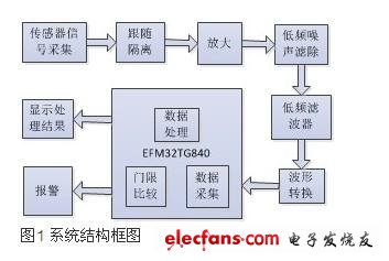
As shown in Figure 1, the pulse signal detected from the sensor is converted into a voltage signal and sent to the voltage follower, which acts as a buffer to isolate the front stage and the rear stage to avoid mutual interference. The output signal is sent to a high-pass filter after pre-amplification to filter out the thermoelectric interference of the sensor, and then passes through a low-pass filter to filter out high-frequency interference in the environment. The processed signal is sent to the subsequent stage to continue to be amplified in order to obtain a small and clear signal. This signal is rectified by the comparator and diode and sent directly to the single-chip processor to drive the display circuit and the alarm circuit.
1. Voltage following and preamplifier circuit
The input signal of the voltage follower, that is, the pulse sensor signal is input from the V + terminal, and the feedback resistance is set to zero, forming an in-phase follower, which acts as a buffer and isolates the influence of the front and rear stages. The function of the heart sound pulse amplifier is to amplify the mV level heart sound signal to the V level for display and recording.
According to the characteristics of heart sound pulse signal, the amplifier is required to have the following characteristics:
High enough gain, about 800 times. Appropriate frequency bandwidth (0.78 ~ 3.33Hz) Because the heart sound pulse signal is weak, the interference and noise are relatively large, the circuit requires a high input impedance to reduce signal loss, and a high common mode rejection ratio (greater than 80dB) to suppress interference And noise.
Because in practical applications, interference from external signals, and considering the stability of the amplifier, the first-stage amplifier cannot achieve such a large gain, so the voltage amplifier is generally composed of two stages. Among them, the front stage uses a negative feedback differential amplifier circuit to improve the common mode signal rejection ratio. The key to this part is how to suppress all kinds of noise and avoid letting noise into the subsequent circuit. Therefore, in the system, the micro-power instrumentation amplifier LM358 based on the dual op amp circuit is used as the preamplifier of the heart sound pulse signal. In order to prevent non-linear distortion and damage the common mode rejection ratio of the circuit, the amplification factor of this part should not be too high, and it is selected to be about 1000 times.

Figure 2 Voltage follow and preamplifier circuit
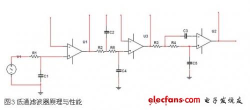
2. High and low pass filter circuit
In this design, the signal frequency is low, between 0.78 ~ 3.33Hz, so the design of the filter becomes the key to this circuit. First, a 0.5 Hz high-pass filter is passed to filter out the thermoelectric interference of the sensor, and then a low-pass filter is passed to filter out most of the interference of the heart sound signal. In the implementation circuit, the ordinary filter has been difficult to filter such a low signal, so the Butterworth filter with a flat gain change is used in this design. Among them, the high-pass is a second-order Butterworth filter, and the low-pass is a Butterworth filter with a cut-off frequency of 5 Hz. Figure 3 is a schematic diagram of low-pass filtering.
After the heart sound signal is amplified by the pre-stage, the amplitude has not yet reached the ideal application value, and there is still some interference, so the post-stage amplifier needs to continue to be amplified to meet the use requirements. The entire circuit uses a general reverse amplifier module circuit.
The function of the comparative rectifier circuit is to convert the processed signal into a square wave without negative pulses, which is sent to the single-chip microcomputer for processing. The circuit consists of a zero-crossing comparator and a rectifier circuit. Since the signal sent to the single-chip microcomputer requires a positive voltage, after the rectifier circuit, the signal will all be converted into a square wave with a positive edge.
Wireless Bluetooth headphone , stereo bluetooth Headphone
Main features
1.Vibration reminding when phone call comes in.
2.rubbish finish with Detachable cable
3.Delivers enhanced audio and bass response and a host of calling features in a sleek, comfortable design.4.Unique, provides all day comfort and ease of use.
5.High quality Bluetooth Headset with music & phone functions.
6. Gift box packing per pc

Wireless Bluetooth Headphones,Wireless Headphones,Wireless Earphones,Wireless Bluetooth Earbuds
Shenzhen Greater Industry Co., Ltd. , https://www.szgreater.net