Synchronous rectification is a new technology that uses a dedicated power MOSFET with very low on-resistance to replace the rectifier diode to reduce rectification losses. It can greatly improve the efficiency of the DC/DC converter and there is no dead zone voltage caused by the Schottky barrier voltage.
Basic Circuit Structure of Synchronous Rectification Power MOSFETs are voltage-controlled devices that have a linear relationship in volt-ampere characteristics during turn-on.
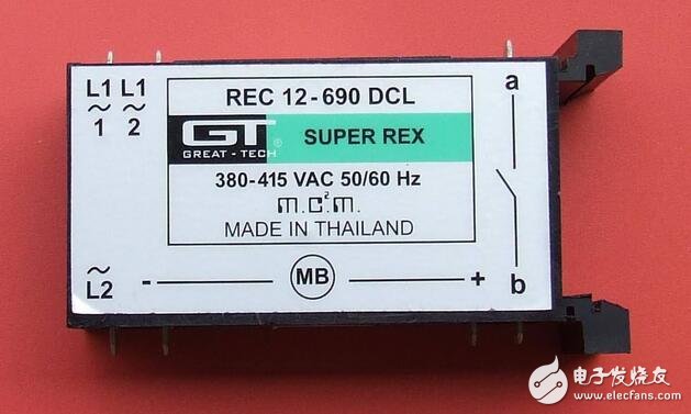
When using a power MOSFET as a rectifier, it is required that the gate voltage must be synchronized with the phase of the rectified voltage to complete the rectification function, so it is called synchronous rectification. PS7516 and PS7616 are lithium battery boost output 5V1A, 2A synchronous rectification boost classic IC, FP6717, FP6716 is also the leader in lithium battery boost output 5V3A, 5V2A.
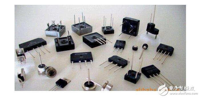
Why should the application of synchronous rectification technology develop electronic technology, making the operating voltage of the circuit lower and lower, and the current is getting larger and larger. Low-voltage operation helps to reduce the overall power consumption of the circuit, but it also poses new challenges for power supply design. The loss of the switching power supply is mainly composed of three parts: the loss of the power switch tube, the loss of the high frequency transformer, and the loss of the rectifier at the output end. In the case of low voltage and high current output, the conduction voltage drop of the rectifier diode is high, and the loss of the rectifier at the output end is particularly prominent. Fast recovery diode (FRD) or ultra-fast recovery diode (SRD) can reach 1.0-1.2V, even with a low-dropout Schottky diode (SBD), it will produce a voltage drop of about 0.6V, which leads to increased rectification losses. Large, power efficiency is reduced.
For example, notebook computers generally use a 3.3V or even 1.8V or 1.5V supply voltage, and can consume up to 20A. At this point, the rectification loss of the ultrafast recovery diode is close to or even exceeds 50% of the power output. Even with Schottky diodes, the loss on the rectifier will reach (18% to 40%) PO, accounting for more than 60% of the total power loss. Therefore, the traditional diode rectification circuit can not meet the needs of achieving high efficiency and small volume of low-voltage, high-current switching power supply, and becomes a bottleneck restricting the efficiency of the DC/DC converter.
Synchronous rectification is better understood than traditional Schottky rectification technology: both rectifiers can be viewed as a gate through which current flows through the gate for load. The traditional rectification technology is similar to a door that must be pushed by someone to push it open. Therefore, every time the current passes through the door, it has to work hard, and it is sweating, and the loss is naturally quite a lot.
The synchronous rectification technology is similar to the induction door of the higher-end venue we passed: it seems to be closed, but when you go to it and need to pass it, it will open itself, and you don’t have to push it yourself. So naturally there is no loss. Through the above analogy, we can know that the synchronous rectification technology greatly reduces the rectification loss at the output end of the switching power supply, thereby improving the conversion efficiency and reducing the heating of the power supply itself.
In high-power power supplies, the consumption of MOS devices is critical. It is likely to be related to the overall efficiency of the power supply. In the previous article, Xiaobian introduced some methods of power dissipation. In this article, Xiaobian will introduce you to the knowledge about the dissipation of synchronous rectifiers and the dissipation of switching MOSFETs.
What is a synchronous rectifier? How is its power consumption? Synchronous rectifier dissipationFor all loads except the maximum load, the drain-source voltage of the MOSFET of the synchronous rectifier is clamped by the capture diode during the on and off periods. Therefore, the synchronous rectifier does not cause switching losses, making its power dissipation easy to calculate. Need to consider only the resistance dissipation.
In the worst case, the loss occurs when the synchronous rectifier has the highest load factor, that is, when the input voltage is at its maximum. By using the RDS(ON)HOT and load factor of the synchronous rectifier and Ohm's law, an approximation of the power dissipation can be calculated:
PDSYNCHRONOUSRECTIFIER=[ILOAD2&TImes;RDS(ON)HOT]&TImes;[1》-)]
Dissipation of switching MOSFETThe calculation of the switching MOSFET resistance loss is similar to the calculation of the synchronous rectifier, using its (different) load factor and RDS(ON)HOT: PDRESISTIVE=[ILOAD2×RDS(ON)HOT]×(VOUT/VIN)
Switching MOSFET switching losses are difficult to calculate because it relies on many factors that are difficult to quantify and often do not affect the specification. A rough approximation is used in the following formula as a first step in evaluating a MOSFET and its performance is verified in the laboratory in the future: PDSWITCHING = (CRSS × VIN2 × fSW × ILOAD) / IGATE.
Where CRSS is the reverse conversion capacitance of the MOSFET (a performance parameter), fSW is the switching frequency, and IGATE is the source of the sink current of the MOSFET gate drive at the startup threshold of the MOSFET (VGS of the flat portion of the gate charge curve) Extreme current.
Once the cost reduction (the cost of the MOSFET is a very important function of the generation that belongs to it) narrows the selection to a specific generation of MOSFETs, the smallest power dissipation in that generation is the model with equal resistance loss and switching loss. . If a smaller (faster) device is used, the increase in resistive losses is greater than the reduction in switching losses.
In devices with larger [RDS(ON) low], the increase in switching loss is greater than the reduction in resistance loss.
If VIN is changing, the power dissipation of the switching MOSFET at VIN(MAX) and VIN(MIN) must be calculated simultaneously. In the worst case MOSFET power dissipation will occur at the minimum or maximum input voltage. Dissipation is the sum of two functions: maximum resistance dissipation at VIN(MIN) (higher load factor) and maximum switching dissipation at VIN(MAX) (due to VIN2). The ideal choice is slightly equal to the dissipation at the VIN extreme, which balances the resistance dissipation and switching dissipation in the VIN range.
If the dissipation at VIN(MIN) is significantly higher, the resistance loss is dominant. In this case, consider using larger switching MOSFETs, or multiple in parallel to achieve lower RDS(ON) values. However, if the dissipation at VIN(MAX) is significantly higher, consider reducing the size of the switching MOSFET (if multiple devices are used, or the MOSFET can be removed) to allow faster switching.
Change the title setting. For example, resetting the input voltage range; changing the switching frequency can reduce switching losses and may make larger, lower RDS(ON) value switching MOSFETs possible; increase gate drive current and reduce switching losses. The MOSFET itself ultimately limits the internal gate resistance of the gate drive current, effectively limiting this approach; using improved MOSFET technology that can switch faster and with lower RDS(ON) values ​​and lower gate resistance .
Due to the limited range of component choices, it may not be possible to accurately adjust the MOSFET size beyond a certain point. The bottom line is that the MOSFET must be dissipated in the worst case.
This article mainly introduces two ways to dissipate MOS devices in high-power power supplies. Through the explanation of these two methods, everyone can understand some of the key points in detail.
1.2 Inch Fnd Numeric Display,Indoor Fnd Numeric Display,Single Digit Fnd Numeric Display,1 Digit Fnd Numeric Display
Wuxi Ark Technology Electronic Co.,Ltd. , https://www.arkledcn.com