The use of voice coding technology can effectively reduce the amount of information storage and improve channel utilization. The mixed excitation linear prediction (MELP) speech coding algorithm can provide higher speech quality, naturalness and clarity at a lower bit rate, and has become the new 2.4 Kb / s speech coding standard of the US Department of Defense. Speech coding technology plays an increasingly important role in today's digital communications, especially in wireless systems.
The Nios II processor is a 32-bit reduced instruction processor soft core introduced by Intel for Altera. Load Nios II soft core and corresponding peripheral interface and custom instructions corresponding to the definition in the software SOPC launched by Altera Corporation to synthesize the design and download to FPGA to easily implement an embedded processing with high-speed DSP function器 [1].
Complex algorithms implemented by hardware are usually more efficient than software. Using custom instructions from Altera ’s Nios II embedded processor, user-defined functions can be added directly to the arithmetic logic unit (ALU) of the Nios II CPU to speed up the execution of special tasks. The advantage of the custom instructions is that the bottleneck part of the program code can be supported by hardware instructions, and the custom instructions can accelerate the program.
1 Composition of MELP
The sampling rate of the MELP vocoder is 8 kHz, each sample value is quantized with 16 bits, each 180 samples is 1 frame, the frame length is 22.5 ms, the number of quantization bits per frame is 54 bits, and the total rate is 2.4 Kb / s.
MELP vocoder is based on the traditional binary excitation LPC model, using 5 new technologies such as mixed excitation, non-periodic pulse, adaptive spectral enhancement, pulse shaping filter and Fourier series amplitude value to make the synthesized speech Can better fit natural speech. Figure 1 shows the MELP codec block diagram [2]. 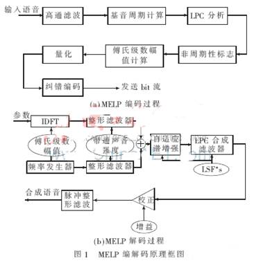
2 Nios II can embed the characteristics of soft core
Nios embedded processor is a user-configurable general-purpose RISC embedded processor. It is a very flexible and powerful processor, so it has become the most popular embedded processor in the world [3]; using an improved Harvard memory structure CPU with separate data and program memory bus control. The SOPC Builder system development tool allows users to easily specify the connection between the Avalon controller and slave devices in the system. These slave devices can be memory or peripheral devices.
The Nios instruction bus is 16 bits and is used to read instructions from memory. The Nios data bus width is 16-bit or 32-bit, which is used for 16-bit or 32-bit configuration of Nios CPU, respectively.
2.1 Command system
The Nios instruction system supports C and C ++ program compilation, including arithmetic and logical operations, bit operations, byte reads, data transfer, flow control, and conditional transfer instructions. The instruction system contains rich addressing modes to reduce code length and improve processor performance.
2.2 Register group
The Nios CPU has a large-capacity windowed general-purpose register set, 8 control registers, a program counter, and a K register for the instruction prefix. The general-purpose register is 16 bits in a 16-bit Nios CPU and 32 bits in a 32-bit Nios CPU. The register set can be configured to contain 128, 256 or 512 registers. The software can access these registers through a sliding window that contains 32 registers. The moving interval of the sliding window is 16 registers, and allows rapid register switching, speeding up subprogram calls and returns.
2.3 Cache
The configurable Nios CPU can optionally contain instruction and data caches. The cache usually improves the performance of the CPU by providing a local storage system, which can quickly respond to bus events generated by the CPU. The implementation of Nios cache is to use a simple direct mapping continuous write structure, this structure design can obtain the maximum performance with the least device resources [4].
2.4 Interrupt handling
The Nios processor allows up to 64 vectored interrupts. There are three types of interrupt sources: external hardware interrupts, internal interrupts, and software interrupts. Nios interrupt processing mode can accurately handle all internal interrupts.
The user can selectively disable the software interrupt, hardware interrupt and internal interrupt of the TRAP instruction. This option can reduce the size of the Nios system, but only for systems where the processor does not run complex software.
2.5 Hardware acceleration
Nios command system can use hardware to improve system performance. Special cycle-intensive software operations can significantly improve system performance with hardware. This feature is provided by modifying the instruction system [5].
Nios processor has two kinds of instruction system modification methods: custom instructions and standard CPU options [6].
2.5.1 User-defined commands
Developers can speed up time-critical software algorithms by adding custom instructions to the Nios processor instruction system, or they can use custom instructions to perform complex processing tasks in single-cycle and multi-cycle operations. In addition, the custom instruction logic circuit added by the user can access the memory and logic circuit outside the Nios system.
Complex operation sequences can be simplified to the execution of single instructions in hardware. This feature allows developers to optimize their software for digital signal processing (DSP), packet header processing, and computationally intensive operations.
Altera's SOPC Builder software provides a graphical user interface (GUI). Developers can use the GUI to add up to five custom instructions to the Nios embedded processor.
2.5.2 Standard CPU options
Altera provides separate pre-defined instructions to improve software performance. The MUL and MSTEP instructions are predefined instructions that are implemented together with other hardware. When the user selects these CPU options in SOPC Builder, the relevant logic is added to the arithmetic logic operation unit (ALU). For example, if the user chooses to execute the MUL instruction, the integer multiplier is automatically added to the ALU of the CPU, and the 16-bit and 16-bit multiplication operations are completed in 2 clock cycles (the same operation is required if the cyclic software program is used to achieve 80 clock cycles).
3 Hardware composition of MELP speech coding
The hardware circuit board uses Altera's FPGA chip EP2C8 as the main control chip, and also includes: 8 MB capacity SDRAM, 2 MB capacity Flash, WM8731 audio chip, comes with audio D / A, A / D, for easy debugging, Also comes with a serial port. The hardware structure of MELP speech coding is shown in Figure 2. 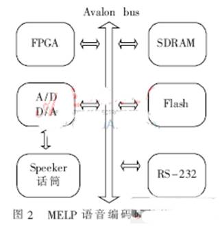
In order to facilitate the debugging of the program, the RS-232 serial port is expanded, which can be directly connected with the computer serial port. The 8 MB capacity SDRAM can provide the storage space required for the Nios II soft core processor to run the embedded operating system, and the 2 MB capacity Flash can also provide storage space for the MELP software compilation. The WM8731 audio chip provides a fast audio codec data stream, and transmits the decoded data stream to the speaker.
WM8731 is a low-power stereo Codec chip, which integrates the headphone amplifier function. Therefore, WN8731 can also be used in MD, DAT and other devices [7]; built-in 24 bit (mulTI-bit) Σ-Δ triangular modulus For conversion and digital-to-analog conversion, both ADC and DAC use super-sampling digital interpolation technology; the number of digital audio supports can be 16 bit to 32 bit, and the sampling rate is from 8 kHz to 96 kHz; stereo audio output with data buffer and digital Volume adjustment, WM8731 is controlled by 2 ~ 3 serial interfaces and can work in master-slave mode. The ADC can achieve a signal-to-noise ratio of 90 dB at a signal voltage of 3.3 V, and the ADC can achieve a signal-to-noise ratio of 85 dB at a signal voltage of 1.8 V. The signal-to-noise ratio of the DAC at a signal voltage of 3.3 V can reach 100 dB, and the signal-to-noise ratio of the DAC at a signal voltage of 1.8 V is also 95 dB. The frequency response of the ADC and DAC is between 8 kHz and 96 kHz, and the high-pass filtering of the ADC can be selectively used. In general, WM8731 is used in the field of professional sound cards.
The interconnection between each chip is connected to the IO pin of FPGA through a lead. The internal bus of the Nios II processor is connected to IO through defined pins, so that the chip that needs to be connected to the Avavon bus can be connected to the bus through the IO pin. Figure 3 shows the connection between the WM8731CODEC chip and the main chip FPGA. 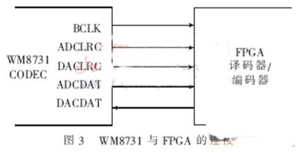
For the serial port, SDRAM and Flash use the soft IP based on the Avalon bus that comes with Nios II.
This paper discusses the hardware structure of FPGA implementation of MELP mixed linear code excitation, introduces the main hardware components of the chip and the main framework of MELP codec, which can be used in the next step of software program compilation.
Jewelry Safe is a secure and protective storage container against burglar & drilling
Details:
A Jewellery Safes are of elegant and top grade appearance and are decoration art in household;
Electronic and fingerprint panels are available;
Higher security performance to secure treasures;
3 wrong code inputs shall trigger the alarm;
Comes with an Emergency power supply in case of an emergency when there is a black out or the electricity is off; a warning tone goes off when the electricity is about to power off, so the owner can change to the emergency power supply in time.
Jewelry Safe
Jewelry Safe,Mechanical Jewelry Safe Box,Jewelry Safe Box,Jewelry Safety Box
YONGFA INTELLIGENT TECHNOLOGY SECURITY CO., LTD. , http://www.yongfa-safe.com