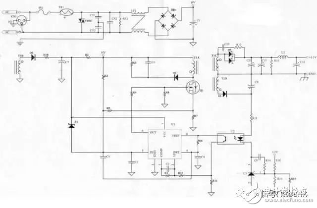
The Iin value is calculated by the transformer. With the Iin value (0.42A), it is known that the company's shared material 2A/250V is used. When designing, the Iin when Pin(max) is considered will exceed the fuse rating.
TR1 (Thermistor)At the moment of power-on, the Iin current is very large due to the short circuit of C1 (primary side filter capacitor). Although the time is very short, it may also cause damage to Power. Therefore, a thermistor must be added before the filter capacitor to limit the boot. Instant Iin is within Spec (115V/30A, 230V/60A), but the thermistor will also consume power, so do not put too much resistance (otherwise it will affect the efficiency), generally use 5Ω-10Ω thermal, if If the C1 capacitor uses a large value, it must be considered to increase the resistance of the thermistor (usually used on a large wattage Power).
VDR1 (surge absorber)When a lightning strike occurs, the parts may be damaged, which may affect the normal operation of the Power. Therefore, it is necessary to protect the Power (usually commonly used 07D471K) by adding a surge absorber to the AC input (after Fuse), but if there is a price Considerations can be ignored first.
CY1, CY2 (Y-Cap)Y-Cap can be generally divided into Y1 and Y2 capacitors. If AC Input has FG (3 Pin), Y2-Cap is generally used. If AC Input is 2Pin (only L, N), Y1-Cap, Y1 and Y2 are generally used. In addition to the price (Y1 is more expensive), the insulation level and withstand voltage are different (Y1 is called double insulation, the insulation withstand voltage is about twice that of Y2, and there will be a "back" symbol on the body of the capacitor or indicate Y1) This circuit è›è ªG, so use Y2-Cap, Y-Cap will affect EMI characteristics, generally the bigger the better, but the leakage and price issues must be considered, leakage (Leakage Current) must meet the safety requirements (3Pin company standard 750uA max).
CX1 (X-Cap), RX1X-Cap is a EMI-resistant part. EMI can be divided into two parts: Conduction and Radiation. The Conduction specification can be divided into two types: FCC Part 15J Class B and CISPR 22 (EN55022) Class B. The FCC test frequency is 450K~30MHz. CISPR 22 test frequency is 150K~30MHz, Conduction can be verified by spectrum analyzer in the factory, Radiation must be verified in the laboratory, X-Cap is generally effective for EMI control in low frequency range (between 150K and M). The larger the X-Cap, the better the EMI control effect (but the higher the price). If the X-Cap is above 0.22 uf (including 0.22 uf), the safety regulations must have a bleeder resistor (RX1, generally 1.2). MΩ 1/4W).
LF1 (Common Choke)EMI control parts mainly affect the middle and low frequency bands of Conduction. The EMI characteristics and temperature rise must be considered at the same time. In the same size of Common Choke, the number of coils is larger (relative wire diameter is finer), EMI prevention The better the effect, but the temperature rise may be higher.
BD1 (rectifier diode)The AC power supply is converted to DC by full-wave rectification, and the Iin value calculated by the transformer is known to be as long as 600V is used because the rectifier diode of 1A/600V is used.
C1 (filter capacitor)The size (capacitance value) of C1 can determine the value of Vin(min) in the calculation of the transformer. The larger the capacitance, the higher the Vin(min) but the higher the price. This part can actually verify whether Vin(min) is in the circuit. Correct, if the AC Input range is 90V~132V (Vc1 voltage is up to about 190V), you can use a capacitor with 200V; if the AC Input range is 90V~264V (or 180V~264V), the Vc1 voltage is about 380V, so it must be Use a capacitor with a withstand voltage of 400V.
D2 (auxiliary power supply diode)Rectifier diodes, commonly used FR105 (1A/600V) or BYT42M (1A/1000V), the main difference between the two:
Different withstand voltage (it does not matter if you use the difference here)
VF is different (FR105=1.2V, BYT42M=1.4V)
R10 (auxiliary power supply resistor)Mainly used to adjust the VCC voltage of the PWM IC. In the current 3843, the VCC must be greater than 8.4V (Min. Load) when designing, but in order to consider the output short circuit, the VCC voltage cannot be designed too high, so as not to be The output is not protected when it is shorted (or the input wattage is too large).
C7 (filter capacitor)The filter capacitor of the auxiliary power supply provides a stable DC voltage of the PWM IC, and generally uses a 100uf/25V capacitor.
Z1 (Zener diode)When the protection circuit fails, the output voltage will rise when the feedback fails, and the auxiliary power supply voltage will increase relatively. If there is no protection circuit, the parts may be damaged. If a Zener is added between the 3843 VCC and the 3843 Pin3. Diode, when the feedback fails, the Zener Diode will collapse, so that Pin3 will reach 1V in advance, which can limit the output voltage and protect the parts. The value of Z1 depends on the level of the auxiliary power supply. The decision of Z1 must also consider whether Exceeding the VGS withstand voltage of Q1, in principle, the company's existing materials (usually 1/2W can be used).
R2 (starting resistor)Provide the path for the first start of 3843. When the first start, charge C7 through R2 to provide the voltage required by 3843 VCC. When the resistance of R2 is large, the turn on time is longer, but the number of Pin watts in short circuit. Smaller, when the resistance of R2 is smaller, the turn on time is shorter, and the number of Pin watts is larger when short circuited, generally using 220KΩ/2W MO.
R4 (Line Compensation)For high and low voltage compensation, the 3843 Pin3 pin is close to 90V/47Hz and 264V/63Hz (usually between 750KΩ~1.5MΩ and 1/4W).
R3, C6, D1 (Snubber)These three parts make up Snubber, the purpose of adjusting Snubber: 1. When there is Spike generated when Q1 off, adjusting Snubber can ensure that Spike will not exceed the withstand voltage value of Q1. 2. Adjusting Snubber can improve EMI. Generally speaking, D1 Using 1N4007 (1A/1000V) EMI characteristics will be better. R3 uses 2W MO resistors, and the withstand voltage of C6 is based on the actual differential pressure at both ends (usually using ceramic capacitors with a withstand voltage of 500V).
Q1 (N-MOS)Currently used are 3A/600V and 6A/600V. The 6A/600V RDS(ON) is smaller than 3A/600V, so the temperature rise will be lower. If the IDS current does not exceed 3A, it should be 3A/600V first. Consider and verify with the temperature rise record, because the price of 6A/600V is much higher than 3A/600V, the use of Q1 also needs to consider whether the VDS exceeds the rated value.
R8The role of R8 is to protect Q1 from Q1.
R7 (Rs resistance)3843 Pin3 pin voltage is up to 1V, R7 size must be matched with R4 to achieve high and low voltage balance. Generally use 2W MO resistor. When designing, first decide R7 and then add R4 compensation. Generally, the 3843 Pin3 pin voltage is designed in Between 0.85V and 0.95V (depending on the wattage, if the wattage is small, it should not be too close to 1V, so as not to reach 1V due to part error).
R5, C3 (RC filter)Filter out the noise of 3843 Pin3 pin. R5 generally uses 1KΩ 1/8W. C3 generally uses 102P/50V ceramic capacitor. If C3 uses less capacitance value, heavy load may not be turned on (because 3843 Pin3 instantly tops to 1V) If the value of the capacitor is larger, there may be a problem that the light load does not turn on and the short circuit is too large.
R9 (Q1 Gate resistance)The size of the R9 resistor will affect the EMI and temperature rise characteristics. Generally, the resistance is large, the Q1 turn on / turn off is slower, and the EMI characteristics are better, but the Q1 has a higher temperature rise and lower efficiency (mainly Because the turn off speed is slower; if the resistance is small, Q1 turn on / turn off is faster, Q1 has lower temperature rise and higher efficiency, but EMI is worse, generally use 51Ω-150Ω 1/8W.
R6, C4 (control oscillation frequency)Determine the working frequency of 3843, the working frequency composed of R and C can be obtained from Data Sheet, C4 is generally 10nf capacitor (error is 5%), R6 uses precision resistor, take DA-14B33 as an example, C4 uses 103P/50VPE capacitor, R6 is a 3.74KΩ 1/8W precision resistor with an oscillation frequency of approximately 45 KHz.
C5The function is similar to RC filter. The main function is to make the high voltage and light load less oscillating. Generally, 101P/50V ceramic capacitor is used.
U1 (PWM IC)3843 is a kind of PWM IC. The Photo Coupler (U2) feedback signal controls the size of the Duty Cycle. Pin3 has a current limiting function (maximum voltage 1V). Currently used 3843, there are KA3843 (SAMSUNG) and UC3843BN ( ST) two kinds, the two feet are the same, but the oscillation frequency is slightly different, UC3843BN is about 2KHz faster than KA3843, the increase of fT will cause some problems (such as EMI problem, short circuit problem), because KA3843 is difficult Buy, so when designing a new model, try to use UC3843BN.
R1, R11, R12, C2 (primary loop gain control)There is an Error AMP inside the 3843. R1, R11, R12, C2 and Error AMP form a negative feedback circuit to adjust the stability of the loop gain. Loop gain. Improper adjustment may cause oscillation or output voltage. Incorrect, generally C2 uses vertical laminated capacitors (good temperature retention).
U2 (Photo coupler)The photo coupler mainly converts the signal on the secondary side to the primary side (in the form of current). When the TL431 on the secondary side is turned on, U2 converts the current on the secondary side proportionally to the primary side. At this time, 3843 is turned off by Pin6 (output) output off signal (Low). The reason for using Photo coupler is to meet the safety requirements (the primacy to secondary distance is at least 5.6mm).
R13 (secondary loop gain control)Control the current flowing through the Photo coupler. When the resistance of R13 is small, the current flowing through the Photo coupler is large, the U2 conversion current is large, and the loop gain is fast (need to confirm whether it will cause oscillation). When the resistance of R13 is large, the flow is high. The photo coupler has a small current, the U2 conversion current is small, and the loop gain is slow. Although it is less likely to cause oscillation, it is necessary to pay attention to whether the output voltage is normal.
U3 (TL431), R15, R16, R18Adjust the output voltage, the output voltage can not exceed 38V (because TL431 VKA is up to 36V, if you add Photo coupler VF value, then Vo should be safer below 38V), TL431 Vref is 2.5V, R15 and R16 are connected in parallel The purpose is to make the output voltage fine-tuned, and the value of R15 and R16 in parallel should not be too large (as much as possible below 2KΩ), so as to avoid output inaccuracy.
R14, C9 (secondary loop gain control)Control the loop gain of the secondary side. Generally, the amplification of the capacitor will slow down the gain; the small capacitance will make the gain faster, the characteristic of the resistor is just opposite to the capacitance, the gain of the resistance amplification becomes faster; the gain of the resistor is slower. As for what is the best value for gain adjustment, you can measure it with Dynamic load to get an optimal value.
D4 (rectifier diode)Since the output voltage is 3.3V, and the Output Voltage Regulator uses TL431 (Vref=2.5V) instead of TL432 (Vref=1.25V), it is necessary to add a set of windings to provide the Photo coupler and TL431. Power supply, because the current required by U2 and U3 is not large (about 10mA), the diode withstand voltage of 100V can be used, so only use 1N4148 (0.15A/100V).
C8 (filter capacitor)Since the current required for U2 and U3 is not large, it is only necessary to use 1u/50V.
D5 (rectifier diode)Output rectifier diode, the use of D5 needs to consider:
Current value
Diode withstand voltage
Taking this circuit as an example, the output current is 4A. It is possible to use a 10A diode (Schottky). However, after the point temperature rise verification, it is found that the D5 temperature is too high, so it must be replaced by a 15A diode because the VF of 10A is lower than the VF of 15A. Big. The 40V withstand voltage is verified to be compliant, so the final 15A/40V Schottky is used.
C10, R17 (secondary side snubber)D5 will have a spike at the moment of the cutoff. If the spike exceeds the withstand voltage of the diode (D5), the diode may be broken. The snubber can be adjusted to reduce the voltage of the spike. In addition to the protection diode, the EMI can be improved. R17 generally uses 1/2W resistors. C10 generally uses ceramic capacitors with a withstand voltage of 500V. The process of snubber adjustment (264V/63Hz) should pay attention to whether R17 and C10 will overheat. This should be avoided.
C11, C13 (filter capacitor)For the secondary-stage first-stage filter capacitor, a capacitor with a small internal resistance (LXZ, YXA...) should be used. Whether the capacitor is selected or not can be determined according to the following three points:
Output Ripple voltage is in accordance with specifications
Whether the capacitor temperature exceeds the rated value
Whether the voltage across the capacitor value exceeds the rated value
R19 (false load)Appropriate use of dummy load can make the line more stable, but the resistance of the dummy load should not be too small, otherwise it will affect the efficiency. It should also be noted whether it exceeds the rated value of the resistor (usually only half of the rated wattage is used).
L3, C12 (LC filter circuit)The LC filter circuit is a second-stage filter. Generally, L3 is amplified (larger inductance) without affecting line stability, so C12 can use a smaller capacitance value.
24V Switching Wall Charger

About this item
-
Input: AC 100-240V 50/60Hz; Output: DC 24V Switching wall charger
-
Plug Type: DC Plug 5.5 x 2.1mm;AC Plug US Plug, Cable Length: 1.2m /1.5m
-
Dimensions (WxLxH): 4.7" x 2" x 1.5", Small and lightweight for convenience, portability and storage. Easy to take anywhere!
-
Built-in protection of over current, over voltage, short circuits
-
This Power Adapter can ensures consistent power and reliable performance for your devices. Can work for 5050 3528 LED Strip 3D Printer CCTV Security System LCD Monitor.
24V Switching Wall Charger
About this item
- Input: AC 100-240V 50/60Hz; Output: DC 24V Switching wall charger
- Plug Type: DC Plug 5.5 x 2.1mm;AC Plug US Plug, Cable Length: 1.2m /1.5m
- Dimensions (WxLxH): 4.7" x 2" x 1.5", Small and lightweight for convenience, portability and storage. Easy to take anywhere!
- Built-in protection of over current, over voltage, short circuits
-
This Power Adapter can ensures consistent power and reliable performance for your devices. Can work for 5050 3528 LED Strip 3D Printer CCTV Security System LCD Monitor.
24v wall charger,24v dc adapter,24v ac dc adapter,24v switching adapter,100-240V AC to DC 24V 3A 72W Power Adapter,12W Ac Switching Power Adapter,24V 0.5A Power Supply For Led Lights
Shenzhen Waweis Technology Co., Ltd. , https://www.waweispowerasdapter.com