When choosing an IGBT, designers face some architectural choices that can favor a form of IGBT, such as symmetrical and asymmetrical blocking, in another. This article reviews the design options offered by different IGBT architectures.
This article refers to the address: http://
The insulated gate bipolar transistor (IGBT) is a common choice for motor drive applications due to its high blocking voltage and low cost compared to power MOSFETs with similar voltage ratings. This technology allows for a variable frequency drive that is considered a good design for energy efficient systems.
The IGBT provides the switching capability needed to drive important inverter stages. Typically, a 600 V blocking voltage rating is required to operate the drive mains from 200-240 VAC, with 1200 V favoring 460 VAC applications.
The evolution from the structure of power MOSFET IGBTs in response to the need for increased blocking voltage during the 1980s. This is achieved by adding an additional PN junction to the drain of the MOSFET architecture to form a bipolar transistor structure and an integrated NPNP semiconductor. With the current manufacture of most power transistors, the structure of the transistor is vertical rather than horizontal, and the PNP bipolar transistor described above is placed on the collector side of the back side of the die. An AP or P+ bath containing the source/emitter and gate regions of the N-doped well connection. Current flows through the bath into a relatively wide N-doped drift region into the collector. However, because it has an insulated gate of a MOSFET, the device as a whole maintains voltage control rather than current control. The gain of the interlock bipolar transistor needs to be carefully controlled to suppress operation as an NPNP thyristor.
Although it generally provides a higher voltage isolation ratio of the MOSFET, the architecture of an IGBT means that it cannot be switched fast, which limits the switching frequency used in the inverter, although recent advances in device construction have driven effective switching frequencies. To 100 kHz. The efficiency of the IGBT is increased by the MOSFET's lower on-state voltage drop. In addition, high current densities can be achieved at higher power ratings to achieve cost-effectiveness with smaller chips than equivalent MOSET.
Early methods and IGBTs included a symmetric structure of the design, also known as a reverse blocking architecture. These have both positive and negative blocking capabilities, which are suitable for AC applications such as matrix (AC-AC) converters or three-level inverters. Asymmetric structures only maintain a positive blocking capability, but tend to be more widely used than symmetric structures because they typically provide a lower on-state voltage drop than a symmetric IGBT. The asymmetric structure is suitable for DC applications such as variable speed motor control. However, IGBT's motor control applications often involve inductive loads, and typically hard switches require parallel use of IGBTs with freewheeling diodes to allow reverse current flow in these topologies. However, such diodes typically provide higher performance than equivalent power MOSFET body diodes.
Another difference is between the IGBT punch-through (PT) and the non-punch-through (NPT) architecture. The PT design is primarily used to reduce the isolation voltage and use the N+ region grown in the P+ substrate and collector region. When the device is turned off, the drift in N becomes completely depleted of the carrier, an effect that is entered below the N+ layer, but does not pass through it completely into the collection "passing the punch". The result is a very thin N-region that minimizes the turn-on voltage. The additional N+ layer also improves the switching speed by reducing the number of excess holes that are injected into the P+ substrate. These carriers are being removed quickly when the device is turned off.
Unfortunately, high doping introduces a large amount of IGBTs needed to remove off minority carriers, which increases conversion time and losses in efficiency. This is a major reason for the lower switching frequency compared to the power MOSFET. PT IGBTs are also protected from thermal runaway.
The treaty was developed to avoid major problems in the PT architecture and to remove the N+ buffer layer. However, they have all been carefully designed to avoid allowing the electric field to penetrate all the way through to the current collector. The transistor is typically made up of a different PT device. Instead of on top of the P-doped substrate on the N regions formed by epitaxy, NPT transistors are typically fabricated using an N-doped substrate and grown in the back collector region.
By thinning the wafer to 100 μm or less, it is possible to use a very-lightly doped collector region and still achieve low resistance and high performance. Using a lighter doped reduction, it can be stored as it converts to better switching performance when it is turned on, because when there are fewer carriers needed, the device is switched to the amount of charge that is killed by the device.
The FGP10N60 and FGP15N60 Fairchild Semiconductor utilizes NPT technology to support a range of motor drive applications. They provide short-circuit resistance of up to 10 microseconds, exhibiting a saturation voltage of approximately 2 V at 150 °C to support high switching speeds, and the transistor exhibits a turn-off delay time of just over 55 ns.
Manufacturers such as the International Rectifier moved to a trench structure almost a decade ago. The trench structure not only allows for higher channel densities by reducing the effective diameter of the gate and base regions, it enhances charge injection of the buildup layer, and reduces the effects of parasitic JFETs from the old planar design. For a given switching frequency, the trench structure reduces conduction and switching losses relative to conventional PT and NPT structures. The trench IGBT is now available in a wide range of ratings from many vendors. IR's own range covers the critical 600 V and 1200 V blocking voltage ranges.
In a typical device, the IRGB4060 is a strap-flop soft-recovery reverse diode and provides a turn-off delay time reduced to 95 nanoseconds to support a relatively high switching frequency of 1.55V transistors.
Adding a field termination area to a thin wafer NPT device enables several further improvements in performance. A bit similar to the PT concept, the electric field of the landing, thus allowing the use of thin wafers for the same high breakdown voltage. The emitter efficiency of the backside junction can be increased by controlling the carrier concentration in the two field and p+ collector layers. As a result, the station provides a thinner wafer with faster conversion (saturation) on devices with low VCE.
Field termination technology has made it easier to integrate freewheeling diodes that require many circuits and the IGBT itself. The example falls on the TRENCHSTOP family Infineon Technologies equipment. Many family members form diodes as part of the core IGBT components through which the reverse current is conducted. Applications provided by others, such as motor control by integrated diode-optimized diode technology in the package, such as the IKD06N60RF, support switching speeds of up to 30 kHz for motor control.
IGBT's evolutionary image of TRENCHSTOP process infineon
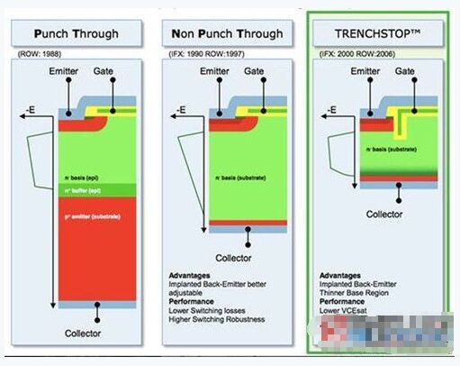
Figure 1: Evolution of the IGBT to the TRENCHSTOP process Infineon.
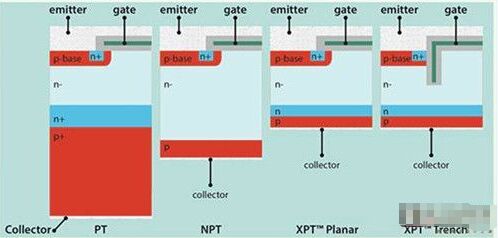
IXYS has developed multiple series of station systems, eventually in the 3rd generation and GEN4 families. The GEN4 architecture combines trench topologies with "extreme light-through" 3rd generation (XPT) field design, supporting a combination of low on-state voltage and fast turn-off to minimize switching losses.
These devices exhibit a square reverse bias safe working area (RBSOA) shape with a breakdown voltage of up to 650 volts and twice the nominal current, at high temperatures, compatible with their bumpless hard switching applications. The device can be packaged with anti-parallel diodes and has a high temperature short circuit robustness at 150 °C for as little as 10 microseconds.
Difference picture between classic and IXYS XPT architecture
Runway Speaker,Runway Micro Speaker,Track Runway Speaker,Outdoor Runway Speakers
NINGBO SANCO ELECTRONICS CO., LTD. , https://www.sancobuzzer.com