Topic content:
This article refers to the address: http://
The electric vehicle brushless motor controller short-circuit working model controller in the short-circuit MOSFET working state calculation MOSFET transient temperature rise calculation formula set short-circuit protection time principle solution:
Temperature rise formula: Tj = Tc + P × Rth(jc)
Determine the allowable short-circuit time based on the thermal resistance coefficient of a single pulse. The higher the operating temperature, the shorter the short-circuit protection time should be.
1 short circuit model and analysis
The short-circuit model is shown in Figure 1, in which only the two phases A and B of the power output stage (a total of three phases) are drawn. Q1 and Q3 are A-phase MOSFETs, Q2 and Q4 are B-phase MOSFETs, and all power MOSFETs are AOT430. L1 is the motor coil and Rs is the current sense resistor.
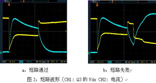
When the controller is working, such as short circuit of the motor, it will form a short-circuit current flowing through Q2, Q3 as shown in Figure 1. The current value is very large, up to several hundred amperes, and the transient temperature rise of the MOSFET is very large. In this case, it should be protected in time, otherwise the MOSFET junction temperature will be too high and the MOSFET will be damaged. The Q3 voltage and current waveforms during short circuit are shown in Figure 2. The MOSFET in Figure 2a can withstand a large current short circuit of 45us, while the MOSFET in Figure 2b cannot withstand a large current short circuit of 45us. When the pulse 45us is turned off, Vds rises. Because the temperature is too high, the MOSFET is shorted only after 10us. Vds drops rapidly and the short-circuit current rises rapidly. From Figure 2, we can see that the peak current reaches 500A during short circuit. This is because the MOSFET directly shorts the positive and negative poles of the power supply during short circuit. The loop impedance is the sum of the wire, the PCB trace and the Rds(on) of the MOSFET. The value is very small. Generally speaking, it is several tens of milliohms to several hundred milliohms.

2 Calculate reasonable protection time
In practical applications, controllers with different designs have different differences in loop inductance and resistance, and different power supply voltages during short circuit. As a result, the short-circuit currents of the three-phase output lines of the controller are different, so the designer should follow Design your own proper circuit and conditions of use to protect your time.
Short circuit protection time calculation steps:
2.1 Calculate the allowable transient temperature rise when the MOSFET is shorted
Because the controller may be suddenly shorted during normal operation, our design should be based on the temperature at normal operation to calculate the allowable transient temperature rise. The junction temperature of the MOSFET can be calculated by:
Tj = Tc + P × Rth(jc)
among them:
Tc: MOSFET surface temperature
Tj: MOSFET junction temperature
Rth(jc): The junction-to-surface thermal resistance can be found in the component Date sheet.
In theory, the junction temperature of the MOSFET cannot exceed 175 °C, so the allowable temperature rise of the MOSFET when the motor phase is shorted is: Trising = Tjmax - Tj = 175-109 = 66 °C.
2.2 Calculate the allowable single-pulse thermal resistance based on transient temperature rise and single-pulse power
It can be seen from Fig. 2 that the power dissipated by the MOSFET during short circuit is about:
P = Vds × I = 25 × 400 = 10000W
The power of the pulse can also be obtained by storing the waveform measured in Figure 2 as EXCEL format data and then integrating it by EXCEL to obtain more accurate pulse power data.
For the MOSFET temperature rise calculation, there is the following formula:
Trising = P × Zθjc × Rθjc
among them:
Rθjc------The junction-to-surface thermal resistance can be found in the component Date sheet.
Zθjc------thermal resistance coefficient
Zθjc = Trising ÷( P × Rθjc)
Zθjc = 66 ÷ (10000 × 0.45) = 0.015
2.3 Determine the allowable short circuit time based on the thermal resistance coefficient of a single pulse
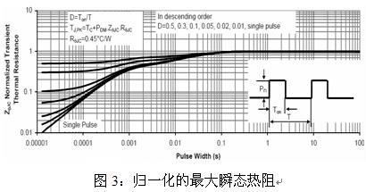
From the bottom curve (single pulse) of Fig. 3, it is known that for a single pulse, to obtain a thermal resistance coefficient of 0.015, the pulse width cannot be greater than 20 us.
3 Several problems should be paid attention to when designing short circuit protection
Since the PCB layout parameters of different controllers are different, the loop impedance is not equal when the phase line is short-circuited, and the short-circuit current is also different. Therefore, different designs of controllers should be designed according to the actual situation of the short circuit protection time.
Since the power supply voltage used in the application may be different, it will also cause different short-circuit currents, which will also affect the protection time.
Pay attention to the maximum possible temperature when the controller is actually working. The higher the operating temperature, the shorter the short-circuit protection time should be.
The short circuit protection time discussed in this article refers to the longest short circuit time that the MOSFET can withstand. When designing a short circuit protection circuit, the response time of the hardware and software should be considered, as well as the peak value of the current protection. These parameters will affect the final protection time. Therefore, hardware circuit design and software writing are crucial.
The short-circuit protection time discussed in this paper is a single-time short-circuit protection time, and cannot be short-circuited again within a short time after short-circuit. If designed as a periodic short circuit protection, the short circuit protection time should be shorter.
4 Conclusion
The short-circuit protection provides reliable and fast protection to the MOSFET at high instantaneous currents, greatly increasing the reliability of the control and reducing the damage rate of the controller.
DBC (Direct Bonded Copper) Substrate is a special process board where copper foil is bonded directly to the surface (single or double sided) of and AI203 OR AIN ceramic substrate at high temperatures and can be etched with various graphics. It has excellent electrical insulation performance, high thermal conductivity, excellent soft brazability, high adhesion strength and a large current-carrying capacity. DBC Substrate mainly used in the fields of rail transit, smart grid, new energy vehicles, industrial frequency conversion, household appliances, military power electronics, wind and photovoltaic power generation.
We custom high precision DBC Substrate with drawings provided by customers. The raw material we use for etched DBC substrate is Ceramic-based double-sided copper clad laminate. We are equipped with professional metal etching equipment and exposure development equipment. Our etching process can achieve double-sided etching of different graphics with 0.3 mm - 0.8mm thickness of copper clad laminate. Also, we can guarantee that our double-sided copper clad laminate substrate is neatly arranged, straight surface line, and have no burr, high product accuracy.
Its superiorities of DBC Substrate are as follow:
1. A ceramic substrate with a coefficient of thermal expansion close to that of a silicon chip, which saves the transition layer of Mo chips, saving labour, material and cost.
2. Excellent thermal conductivity, making the chip package very compact, thus greatly increasing the power density and improving the reliability of systems and devices.
3. A large number of high-voltage, high-power devices have high requirements for heat dissipation, and ceramic substrates have a better heat dissipation effect.
4. Ultra-thin (0.25mm) ceramic substrates can replace beo, without environmental toxicity problems.
5. Large current carrying capacity, 100A continuous current through 1mm wide 0.3mm thick copper body, temperature rise of about 17 ℃; 100A continuous current through 2mm wide 0.3mm thick copper body, temperature rise of only about 5 ℃.
6. High insulation withstand voltage, to ensure personal safety and equipment protection
7. New packaging and assembly methods can be realized, resulting in highly integrated products and reduced size
8. The ceramic substrate is highly resistant to vibration and wear, ensuring its long service life.
High Precision DBC Substrate,Etched DBC Substrate,Double-Sided Copper Clad Laminate Substrate
SHAOXING HUALI ELECTRONICS CO., LTD. , https://www.cnsxhuali.com